
Products Category
- FM Transmitter
- 0-50w 50w-1000w 2kw-10kw 10kw+
- TV Transmitter
- 0-50w 50-1kw 2kw-10kw
- FM Antenna
- TV Antenna
- Antenna Accessory
- Cable Connector Power Splitter Dummy Load
- RF Transistor
- Power Supply
- Audio Equipments
- DTV Front End Equipment
- Link System
- STL system Microwave Link system
- FM Radio
- Power Meter
- Other Products
- Special for Coronavirus
Products Tags
Fmuser Sites
- es.fmuser.net
- it.fmuser.net
- fr.fmuser.net
- de.fmuser.net
- af.fmuser.net ->Afrikaans
- sq.fmuser.net ->Albanian
- ar.fmuser.net ->Arabic
- hy.fmuser.net ->Armenian
- az.fmuser.net ->Azerbaijani
- eu.fmuser.net ->Basque
- be.fmuser.net ->Belarusian
- bg.fmuser.net ->Bulgarian
- ca.fmuser.net ->Catalan
- zh-CN.fmuser.net ->Chinese (Simplified)
- zh-TW.fmuser.net ->Chinese (Traditional)
- hr.fmuser.net ->Croatian
- cs.fmuser.net ->Czech
- da.fmuser.net ->Danish
- nl.fmuser.net ->Dutch
- et.fmuser.net ->Estonian
- tl.fmuser.net ->Filipino
- fi.fmuser.net ->Finnish
- fr.fmuser.net ->French
- gl.fmuser.net ->Galician
- ka.fmuser.net ->Georgian
- de.fmuser.net ->German
- el.fmuser.net ->Greek
- ht.fmuser.net ->Haitian Creole
- iw.fmuser.net ->Hebrew
- hi.fmuser.net ->Hindi
- hu.fmuser.net ->Hungarian
- is.fmuser.net ->Icelandic
- id.fmuser.net ->Indonesian
- ga.fmuser.net ->Irish
- it.fmuser.net ->Italian
- ja.fmuser.net ->Japanese
- ko.fmuser.net ->Korean
- lv.fmuser.net ->Latvian
- lt.fmuser.net ->Lithuanian
- mk.fmuser.net ->Macedonian
- ms.fmuser.net ->Malay
- mt.fmuser.net ->Maltese
- no.fmuser.net ->Norwegian
- fa.fmuser.net ->Persian
- pl.fmuser.net ->Polish
- pt.fmuser.net ->Portuguese
- ro.fmuser.net ->Romanian
- ru.fmuser.net ->Russian
- sr.fmuser.net ->Serbian
- sk.fmuser.net ->Slovak
- sl.fmuser.net ->Slovenian
- es.fmuser.net ->Spanish
- sw.fmuser.net ->Swahili
- sv.fmuser.net ->Swedish
- th.fmuser.net ->Thai
- tr.fmuser.net ->Turkish
- uk.fmuser.net ->Ukrainian
- ur.fmuser.net ->Urdu
- vi.fmuser.net ->Vietnamese
- cy.fmuser.net ->Welsh
- yi.fmuser.net ->Yiddish
How Does A Transistor Work?
The transistor was invented by William Shockley in 1947. A transistor is a three-terminal semiconductor device which can be used for switching applications, amplification of weak signals and in quantities of thousands and millions of transistors are interconnected and embedded into a tiny integrated circuit/chip, which makes a computer memory.
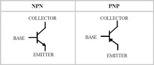
Bipolar Transistor Types
What is Transistor?
The transistor is a semiconductor device that can function as a signal amplifier or as a solid-state switch. The transistor can be considered as two p-n junctions that are placed back to back.
The structure has two PN junctions with a very small base region between the two outlying areas for the collector and emitter. There are three main classifications of transistors each with its own symbols, characteristics, design parameters, and applications.
Bipolar Junction Transistor
BJTs are considered current driven devices and have a relatively low input impedance. They are available as NPN or PNP types. The designation describes the polarity of the semiconductor material used to fabricate the transistor.
The arrow direction shown in the symbol of transistor indicates the direction of current through it. Thus, in NPN type, the current comes out from the emitter terminal. Whereas in PNP, the current goes into the emitter.
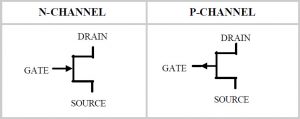
Field Effect Transistors
FET’s, are referred to as voltage driven devices which have a high input impedance. Field Effect Transistors are further sub-classified into two groups, Junction Field Effect Transistors (JFET) and Metal Oxide Semiconductor Field Effect Transistors (MOSFET).
Field Effect Transistors
Similar to the JFET above except the input voltage is capacitive coupled to the transistor. The device has a low power drain but is easily damaged by static discharge.
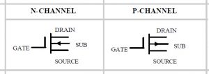
MOSFET( nMOS and pMOS)
IGBT is the most recent transistor development. This is a hybrid device which combines characteristics of both the BJT with the capacitive coupled and the NMOS/ PMOS device with high impedance input.
Insulated Gate Bipolar Transistor (IGBT)
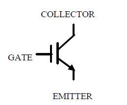
In this article, we will discuss Bipolar transistor working The BJT is a three-lead device with an Emitter, a Collector, and a Base lead. Basically, The BJT is a current driven device. Two P-N junctions exist within a BJT.
One PN junction exists between the emitter and the base region, a second exists between the collector and the base region. A little amount of current flow emitter-to-base (base current measured in micro amps) can control a reasonably large current flow through the device from the emitter to the collector (collector current measured in milliamps).
Bipolar transistors are available in complimentary nature with respect to its polarities. The NPN has an emitter and collector of N-Type semiconductor material and the base material is the P-Type semiconductor material. In PNP these polarities are simply reversed here, the emitter and collector are P-Type semiconductor material and the base is N-Type materials.
The functions of NPN and PNP transistors essentially the same, but the power supply polarities are reversed for each type. The only major difference between these two types is that the NPN transistor has a higher frequency response than the PNP transistor (because the flow of electron is faster than hole flow). Therefore, in high-frequency applications, the NPN transistors are used.
In usual BJT operation, the base-emitter junction is forward biased and the base-collector junction is reverse biased. When a current flows through the base-emitter junction, a current also flows in the collector circuit. This is larger and proportional to the one in the base circuit.
In order to explain the way in which this happens, the example of an NPN transistor is taken. The same principles are used for the p-n-p transistor except that the current carrier is holes rather than electrons and the voltages are reversed.
The emitter of the NPN device is made of an n-type material, hence the majority carriers are electrons. When the base-emitter junction is forward biased the electrons move from the n-type region towards the p-type region and the holes move towards the n-type region.
When they reach each other they combine enabling a current to flow across the junction. When the junction is reverse biased the holes and electrons move away from the junction, now a depletion region forms between the two areas and no current flows.
When a current flows between the base and emitter, electrons leave the emitter and flow into the base, the illustration shown in the above diagram. Generally, the electrons would combine when they reach depletion region.
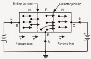
BJT NPN Transistor Biasing Circuit
In this way, they are able to flow across what is effectively a reverse biased junction, and current flows in the collector circuit.
It is found that the collector current is significantly higher than the base current and because the proportion of electrons combining with holes remains the same the collector current is always proportional to the base current.
The ratio of the base to collector current is given the Greek symbol β. Typically the ratio β may be between 50 and 500 for a small signal transistor.
This means that the collector current will be between 50 and 500 times more than that of base region current. For high power transistors, the value of β is probable to be smaller, with figures of 20 not being unusual.
Transistor Applications
1. Most common applications of transistor comprise of analog & digital switches, power regulators, multi-vibrators, different signal generators, signal amplifiers & equipment controllers.
2. Transistors are the basic building blocks of the integrated circuits and most up-to-date electronics.
Maybe you will like:
http://fmuser.net/search.asp?page=1&keys=Transistor&searchtype=
http://fmuser.net/search.asp?keys=MOSFET&Submit=Search
How to Use Signal Generators for Ham Radios