
Products Category
- FM Transmitter
- 0-50w 50w-1000w 2kw-10kw 10kw+
- TV Transmitter
- 0-50w 50-1kw 2kw-10kw
- FM Antenna
- TV Antenna
- Antenna Accessory
- Cable Connector Power Splitter Dummy Load
- RF Transistor
- Power Supply
- Audio Equipments
- DTV Front End Equipment
- Link System
- STL system Microwave Link system
- FM Radio
- Power Meter
- Other Products
- Special for Coronavirus
Products Tags
Fmuser Sites
- es.fmuser.net
- it.fmuser.net
- fr.fmuser.net
- de.fmuser.net
- af.fmuser.net ->Afrikaans
- sq.fmuser.net ->Albanian
- ar.fmuser.net ->Arabic
- hy.fmuser.net ->Armenian
- az.fmuser.net ->Azerbaijani
- eu.fmuser.net ->Basque
- be.fmuser.net ->Belarusian
- bg.fmuser.net ->Bulgarian
- ca.fmuser.net ->Catalan
- zh-CN.fmuser.net ->Chinese (Simplified)
- zh-TW.fmuser.net ->Chinese (Traditional)
- hr.fmuser.net ->Croatian
- cs.fmuser.net ->Czech
- da.fmuser.net ->Danish
- nl.fmuser.net ->Dutch
- et.fmuser.net ->Estonian
- tl.fmuser.net ->Filipino
- fi.fmuser.net ->Finnish
- fr.fmuser.net ->French
- gl.fmuser.net ->Galician
- ka.fmuser.net ->Georgian
- de.fmuser.net ->German
- el.fmuser.net ->Greek
- ht.fmuser.net ->Haitian Creole
- iw.fmuser.net ->Hebrew
- hi.fmuser.net ->Hindi
- hu.fmuser.net ->Hungarian
- is.fmuser.net ->Icelandic
- id.fmuser.net ->Indonesian
- ga.fmuser.net ->Irish
- it.fmuser.net ->Italian
- ja.fmuser.net ->Japanese
- ko.fmuser.net ->Korean
- lv.fmuser.net ->Latvian
- lt.fmuser.net ->Lithuanian
- mk.fmuser.net ->Macedonian
- ms.fmuser.net ->Malay
- mt.fmuser.net ->Maltese
- no.fmuser.net ->Norwegian
- fa.fmuser.net ->Persian
- pl.fmuser.net ->Polish
- pt.fmuser.net ->Portuguese
- ro.fmuser.net ->Romanian
- ru.fmuser.net ->Russian
- sr.fmuser.net ->Serbian
- sk.fmuser.net ->Slovak
- sl.fmuser.net ->Slovenian
- es.fmuser.net ->Spanish
- sw.fmuser.net ->Swahili
- sv.fmuser.net ->Swedish
- th.fmuser.net ->Thai
- tr.fmuser.net ->Turkish
- uk.fmuser.net ->Ukrainian
- ur.fmuser.net ->Urdu
- vi.fmuser.net ->Vietnamese
- cy.fmuser.net ->Welsh
- yi.fmuser.net ->Yiddish
Through Hole vs Surface Mount | What is the Difference?
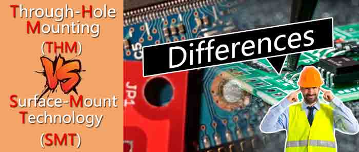
"What are the advantages and disadvantages of Through-Hole Mounting (THM) and Surface-Mount Technology (SMT)? What are the main differences and commons between THM and SMT? And Which is better, THM or SMT? We hereby show you the the differences between Through-Hole Mounting (THM) and Surface-Mount Technology (SMT), let's take a look! ----- FMUSER"
Sharing is Caring!
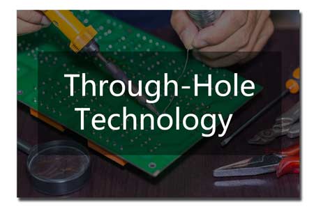
1. Through Hole Mounting | PCB Assembly
1.1 What is THM (Through-Hole Mounting) - Through Hole Technology
1.2 Through Hole Components | What are They and How They Work?
1) Types of Through Hole Components
2) Types of Plated Through Hole Components (PTH)
3) Types of Plated Through-hole Circuit Board Components
2. Through Hole Components | What are the Advantages of THC (Through Hole Components)
3. Surface Mount Technology | PCB Assembly
4. SMD Components (SMC) | What are They and How They Work?
5. What is the Difference between THM and SMT in PCB Assembly?
6. SMT and THM | What are the Advantages and Disadvantages?
1) Advantages of Surface Mount Technology (SMT)
2) Disadvantages of Surface-Mount Technology (SMT)
3) Advantages of Through-Hole Mounting (THM)
4) Disadvantages of Through-Hole Mounting (THM)
7. Frequently Asked Questions

FMUSER is the expert in manufacturing High-frequency PCBs, we provide not only budget PCBs, but also online support for your PCBs design, contact our team for more information!
1. Through Hole Mounting | PCB Assembly
1.1 What is THM (Through-Hole Mounting) - Through Hole Technology
THM refers to "Through-Hole Mounting" which is also called "THM", "thru-hole", "through hole" or "through hole technology", "THT". As what we introduced in this page, through hole Mounting is the process by which component leads are placed into drilled holes on a bare PCB, it is kind of the predecessor of Surface Mount Technology.
Over the past few years, the electronic industry has witnessed a steady rise, owing to the increasing use of electronics in various facets of human life. As demand for advanced and miniature products grows, so does the printed circuit board (PCB) industry.
There are also many PCB terminology in PCB manufacturing, PCB design, and etc. You might have a better understanding of printed circuit board after reading some of the PCB terminologies from the below page!
Also read: What is Printed Circuit Board (PCB) | All You Need to Know
For years, through-hole technology was utilized in the construction of nearly all printed circuit boards (PCBs). While through-hole mounting provides stronger mechanical bonds than surface-mount technology techniques, the additional drilling required makes the boards more expensive to produce. It also limits the available routing area for signal traces on multilayer boards since the holes must pass through all layers to the opposite side. These issues are just two of the many reasons that surface-mounted technology became so popular in the 1980s.
Through Hole technology replaced early electronics assembly techniques such as point-to-point construction. From the second generation of computers in the 1950s until surface-mount technology became popular in the late 1980s, every component on a typical PCB was a through-hole component.
Today, PCBs are getting smaller than before. Owing to their small surfaces it is challenging to mount various components on a circuit board. To ease this, manufacturers are using two techniques to mount electrical components onto the circuit board. Plated Through-hole Technology (PTH) and Surface Mount Technology (SMT) are these techniques. PTH is one of the most commonly used techniques used to mount electrical components, including microchips, capacitors, and resistors to the circuit board. In through-hole assembly, the leads are threaded through pre-drilled holes to make a crisscross pattern on the other side.
Also read: PCB Terminology Glossary (Beginners-Friendly) | PCB Design
▲ BACK ▲
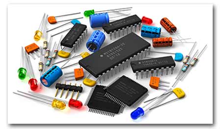
1.2 Through Hole Components | What are They and How They Work?
1) Types of Through Hole Components
Before we starting, there is something you should know about the basic electronic components. Electronic components have two basic types, active and passive. The following are the details of these two classifications.
● Active components
● Passive components
Active component
What is an active electronic component?
Active electronic components are components that can control current. Different types of printed circuit boards have at least one active component. Some examples of active electronic components are transistors, vacuum tubes, and thyristor rectifiers (SCRs).
Example:
Diode - two end components of current in one main direction. It has a low resistance in one direction, and high resistance in the other direction
Rectifier - A device converts AC (change direction) into direct current (in one direction)
Vacuum tube - tube or valve via vacuum conductive current
Function: Active component management current. Most PCBs have at least one active component.
From the perspective of the circuit, the active component has two basic features:
● The active component itself will consume power.
● Except for input signals, external power supplies must also be required to work.
Passive component
What are passive electronic components?
Passive electronic components are those that have no capability to control the current through another electrical signal. Examples of passive electronic components include capacitors, resistors, inductors, transformers, and some diodes. These may be the square hole of the SMD assembly.
Also read: PCB Design | PCB Manufacturing Process Flow Chart, PPT, and PDF
2) Types of Plated Through Hole Components (PTH)
PTH components are known as “through-hole” because the leads are inserted through a copper-plated hole in the circuit board. These components possess two types of leads:
● Axial lead components
● Radial lead components
Axial Lead Components (ALC):
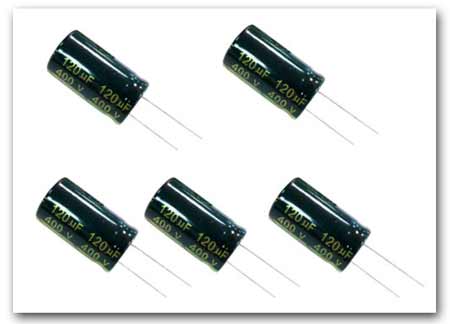
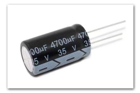
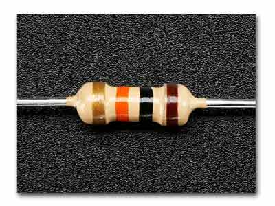
These components may feature a lead or multiple leads. The lead wires are made to exit from one end of the component. During the plated through-hole assembly, both ends are placed through separate holes on the circuit board. Thus, components are closely placed on the circuit board. Electrolytic capacitors, fuses, light-emitting diodes (LEDs), and carbon resistors are a few examples of axial components. These components are preferred when manufacturers are looking for a compact fit.
Radial Lead Components (RLC):
The leads of these components protrude out of their body. Radial leads are mostly used for high-density boards, as they occupy less space on the circuit boards. Ceramic disk capacitors are one of the important types of radial lead components.
Example:
Resistors - Electrical components of both end resistors. The resistor can reduce current, change the signal level, voltage division, and the like.
Capacitors - These components can store and release charge. They can filter the power cord and block the DC voltage while allowing the AC signal to pass.
From the perspective of the circuit, passive components have two basic features:
● The passive component itself consumes electricity or converts the electrical energy into other forms of other energy.
● Only the signal is input, it is not necessary to work properly.
Function - Passive components cannot use another electrical signal to change the current.
By assembly of printed circuit boards, including surface mounting techniques and through holes, these components together constitute a more secure, more convenient process than in the past. Although these components may become more complicated in the next few years, their science behind them is eternal.
Also read: PCB Manufacturing Process | 16 Steps to Make a PCB Board
3) Types of Plated Through-hole Circuit Board Components
And Just like all other components, plated through-hole circuit board components can be roughly divided into:
● Through-hole active components
● Through-hole passive components.
Each type of component mounts to the board in the same way. The designer needs to place through-holes in their PCB layout, where the hols are surrounded with a pad on the surface layer for soldering. The through-hole mounting process is simple: place the component leads into the holes and solder the exposed lead to the pad. Plated through-hole circuit board components are large and rugged enough that they can be easily hand soldered. For passive through-hole components, the component leads can be quite long, so they are often clipped to a shorter length before mounting.
Passive Through-Hole Components
Passive through-hole components come in two possible types of packages: radial and axial. An axial through-hole component has its electrical leads running along the component's axis of symmetry. Think about a basic resistor; the electrical leads run along the cylindrical axis of the resistor. Diodes, inductors, and many capacitors are mounted in the same way. Not all through-hole components come in cylindrical packages; some components, like high power resistors, come in rectangular packages with a lead wire running down the length of the package.
Active Through-hole Components
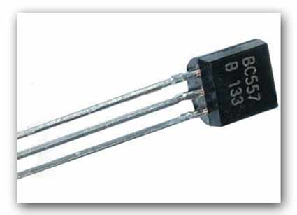
If you remember back to your electronics classes, you'll likely remember the integrated circuits you used with dual-inline package (DIP) or plastic DIP (PDIP). These components are normally seen as being mounted on breadboards for proof-of-concept development, but they are commonly used in real PCBs. The DIP package is common for active through-hole components, such as op-amp packages, low-power voltage regulators, and many other common components. Other components like transistors, higher power voltage regulators, quartz resonators, higher power LEDs, and many others may come in a zig-zag in-line package (ZIP) or transistor outline (TO) package. Just like axial or radial passive through-hole technology, these other packages mount to a PCB in the same way.
Through-hole components came about at a time when designers were more concerned with making electronic systems mechanically stable and were less concerned about aesthetics and signal integrity. There was less of a focus on reducing space taken up by components, and signal integrity problems were not a concern. Later, as power consumption, signal integrity, and board space requirements began to take center stage, designers needed to use components that provide the same electrical functionality in a smaller package. This is where surface-mount components come in.
2. Through Hole Components | What are the Advantages of THC (Through Hole Components)
Through-hole components are best used for high-reliability products that require stronger connections between layers. The through-hole components are still playing important roles in PCB assembly process for these advantages:
● Durability:
Many parts that serve as an interface must have a more robust mechanical attachment than what can be achieved through surface mount soldering. Switches, connectors, fuses, and other parts that will be pushed and pulled by human or mechanical forces, need the strength of a soldered thru-hole connection.
● Power:
Components that are used in circuits that conduct high power levels are usually only available in thru-hole packages. Not only are these parts larger and heavier requiring a more robust mechanical attachment, but the current loads may be too much for a surface mount solder connection.
● Heat:
Components that conduct a lot of heat may also favor a thru-hole package. This allows the pins to conduct heat through the holes and out into the board. In some cases these parts may be bolted through a hole in the board as well for additional heat transfer.
● Hybrid:
These are the parts that are a combination of both surface mount pads and thru-hole pins. Examples would include high-density connectors whose signal pins are surface mount while their mounting pins are thru-hole. The same configuration can also be found in parts that carry a lot of currents or run hot. The power and/or hot pins will be thru-hole while the other signal pins will be surface mount.
Whereas SMT components are secured only by solder on the surface of the board, through-hole component leads run through the board, allowing the components to withstand more environmental stress. This is why through-hole technology is commonly used in military and aerospace products that may experience extreme accelerations, collisions, or high temperatures. Through-hole technology is also useful in test and prototyping applications that sometimes require manual adjustments and replacements.
Also read: How to Recycle A Waste Printed Circuit Board? | Things You Should Know
▲ BACK ▲
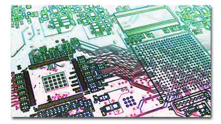
3. Surface Mount Technology | PCB Assembly
What is SMT (Surface Mount) - Surface Mount Technology
Surface-mount technology (SMT) refers to a technology that putting different types of electrical components directly onto a surface of a PCB board, while the surface-mount device (SMD) refers to those electrical components being installed on the printed circuit board (PCB), SMD are also known as SMC (Surface Mount Device Components)
As an alternative to Through-Hole (TH) printed circuit board (PCB) design and manufacturing practices, Surface Mount Technology (SMT) performs better when size, weight, and automation are considerations because of its more efficient PCBs fabricating reliability or quality than the Through-hole mounting technology
This technology has facilitated the application of electronics for functions that were not previously thought of as practical or possible. SMT uses surface-mount devices (SMDs) to replace larger, heavier, and more cumbersome counterparts in the older Through-hole PCB construction.
▲ BACK ▲
4. SMD Components (SMC) | What are They and How They Work?
The SMD components on a PCB board are easy to identify, they have a lot in common, such as the appearance and working methods, here are some of the SMD components on a PCB board, you may meet more you need in this page, but first I would like to show you the following commply used surface mount components:
● Chip Resistor (R)
● Network Resistor (RA/RN
● Capacitor (C)
● Diode (D)
● LED (LED)
● Transistor (Q)
● Inductor (L)
● Transformer (T)
● Crystal Oscillator (X)
● Fuse
Here are basically how these SMD components work:
● Chip Resistor (R)
generally, the three digits on the body of a chip resistor indicate its resistance value. Its first and second digits are significant digits, and the third digit indicates the multiple of 10, such as "103'' indicates "10KΩ", "472" is "4700Ω". The letter "R" means a decimal point, for example, "R15" means "0.15Ω".
● Network Resistor (RA/RN)
which packages several resistors with the same parameters together. The network resistors are generally applied to digital circuits. The resistance identification method is same as the chip resistor.
● Capacitor (C)
the most used are MLCC (Multi-layer Ceramic Capacitors), MLCC is divided into COG (NPO), X7R, Y5V according to the materials, of which COG (NPO) is the most stable. Tantalum capacitors and aluminum capacitors are two other special capacitors that we use, note to distinguish the polarity of them two.
● Diode (D), wide applied SMD components. Generally, on the diode body, the color ring marks the direction of its negative.
● LED (LED), LEDs are divided into ordinary LEDs and high-brightness LEDs, with colors of white, red, yellow, and blue, etc. The determination of LEDs' polarity should be based on a specific product manufacturing guideline.
● Transistor (Q), typical structures are NPN and PNP, including Triode, BJT, FET, MOSFET, and the like. The most used packages in SMD components are SOT-23 and SOT-223 (larger).
● Inductor (L), the inductance values is generally directly printed on the body.
● Transformer (T)
● Crystal Oscillator (X), mainly used in various circuits to generate oscillation frequency.
● Fuse
IC (U), that is, integrated circuits, the most important functional components of electronic products. The packages are more complicated, which will be introduced in detail later.
▲ BACK ▲
5. What is the Difference between THM and SMT in PCB Assembly?
To help you build up a better understanding of the difference between through-hole mounting and surface mounting, FMUSER provides a comparison sheet for reference:
| Difference in | Surface Mounting Technology (SMT) | Through-Hole Mounting (THM) |
|
Space Occupation |
Small PCB Space Occupation Rate |
High PCB Space Occupation Rate |
|
Lead wires requiration |
Direct components mounting, no need for lead wires |
Lead wires are needed for mounting |
|
Pin count |
Much higher |
Normal |
|
Packing density |
Much higher |
Normal |
|
Cost of components |
Less expensive |
Relatively high |
|
Cost of production |
Suitable for high volume production at low costs |
Suitable for low volume production at high costs |
|
Size |
Relatively Small |
Relatively Big |
|
Circuit Speed |
Relatively Higher |
Relatively Lower |
|
Structure |
Complicated in design, production, and technology |
Simple |
|
Range of Application |
Most applied in large and bulky components subjecting to stress or high-voltage |
Not recommended for high-power or high-voltage usage |
In a word, the key differences between thru hole and surface mount are:
● SMT resolves the space problems that are common to through-hole mounting.
● In SMT, components do not have leeds and are directly mounted to the PCB, whereas through-hole components require lead wires that pass through drilled holes.
● The pin count is higher in SMT than in through-hole technology.
● Because components are more compact, the packing density achieved through SMT is much higher than in through-hole mounting.
● SMT components are typically less expensive than their through-hole counterparts.
● SMT lends itself to assembly automation, making it far more suitable for high volume production at lower costs than through-hole production.
● Although SMT is typically cheaper on the production side, the capital required for investing in machinery is higher than for through-hole technology.
● SMT makes it easier to acquire higher circuit speeds because of its reduced size.
● The design, production, skill, and technology that SMT demands is quite advanced as compared to through-hole technology.
● Through-hole mounting is typically more desirable than SMT in terms of large, bulky components, components that are subject to frequent mechanical stress, or for high-power and high-voltage parts.
● Although there are scenarios in which through-hole mounting may still be utilized in modern PCB assembly, for the most part, surface mounted technology is superior.
6. SMT and THM | What are the Advantages and Disadvantages?
You can see the differences from their features mentioned above, but in order to help you make a better understanding of Through-Hole Mounting (THM) and Surface Mount Technology (SMT), FMUSER hereby provides a full comparison list of the advantages and disadvantages of THM and SMT, read the following content about their advantages and disadvantages now!
Qucik View (Click to visit)
What are the Advantages of Surface Mount Technology (SMT)?
What are the Disadvantages of Surface Mount Technology (SMT)?
What are the Advantages of Through-Hole Mounting (THM)?
What are the Disadvantages of Through-Hole Mounting (THM)?
1) What are the Advantages of Surface Mount Technology (SMT)?
● Considerable electrical noise reduction
Most importantly, SMT has significant savings in weight and real estate and electrical noise reduction. The compact package and lower lead inductance in SMT mean Electromagnetic Compatibility, (EMC) will be more easily achievable.
● Realize Miniaturization with a significant reduction in weight
The geometric size and volume occupied by SMT electronic components are much smaller than that of through-hole interpolation components, which can be generally reduced by 60%~70%, and some components can even be reduced by 90% in size and volume.
Meanwhile, the SMT component can weigh as little as one-tenth of their common thru-hole equivalents. Because of this reason a significant decrease in weight of the Surface Mount Assembly (SMA).
● Optimal utilization of board space
SMT components occupy small because of this only one-half to one-third of the space on the printed circuit board. This leads to designs that are more lightweight and compact.
SMD components are much smaller (SMT allows for smaller PCB sizes) than THM components, which means with a more real estate to work with, the overall density (safety density for example) of the board will be increased tremendously. The compact design of SMT also enables higher circuit speeds.
● High Signal Transmission Speed
SMT assembled components are not only compact in structure but also high in safety density. The assembly density can reach 5.5~20 solder joints per square centimeter when the PCB is pasted on both sides. SMT assembled PCBs can realize high-speed signal transmission due to short circuits and small delays.
● Since every electronic part is not accessible in surface mount, the real area reserves on a board will depend on the ratio of through-hole components changed by surface mount parts.
● SMD components can be placed on both sides of a PCB, which means a higher component density with more connections possible per component.
● Good High-Frequency Effects
Because the components have no lead or short lead, the distributed parameters of the circuit are naturally reduced, which enables lower resistance and inductance at the connection, mitigating the undesired effects of RF signals providing better high-frequency performance
● SMT is beneficial to automatic production, improving yield, production efficiency, and lower costs
Using a Pick and Place machine for placing the components will reduce production time as well as lower costs.
The routing of traces is reduced, the size of the board is reduced.
At the same time, because drilled holes are not required for assembly, SMT allows for lower costs and faster production time. During assembly, SMT components can be placed at rates of thousands—even tens of thousands—of placements per hour, versus less than a thousand for THM, the component failure caused by the welding process will also be greatly reduced and the reliability will be improved.
● Minimized material costs
SMD components are mostly cheaper compared to THM components due to the improvement of production equipment efficiency and the reduction of packaging material consumption, the packaging cost of most SMT components has been lower than that of THT components with the same type and function
If the functions on the surface mount board are not expanded, the expanded between inter-package spacings made possible by littler surface mount parts and a decrease in the number of boring gaps may likewise reduce the number of layer counts in the printed circuit board. This will again bring down the board cost.
● Solder joint formation is much more reliable and repeatable using programmed reflow ovens versus through techniques.
SMT has proven to be more stable and better performing in impact-resistance and vibration-resistance, this is of great significance to realize the ultra-high-speed operation of electronic equipment. Despite the apparent advantages, SMT manufacturing presents its own set of unique challenges. While components can be placed more quickly, the machinery required to do so is very expensive. Such high capital investment for the assembly process means that SMT components can push costs up for low volume prototype boards. Surface-mounted components require more precision during manufacturing due to the increased complexity of routing blind/buried vias as opposed to through-hole.
Precision is also important during design, as violations of your contract manufacturer’s (CM’s) DFM pad layout guidelines can lead to mounting issues such as tombstoning, which can significantly reduce the yield rate during a production run.
▲ BACK ▲
● SMT is unsuitable for large, high-power, or high-voltage parts
Generally, the power of SMD Components is Less. Not all Active and Passive Electronic Components are available in SMD, most SMD components are not suitable for high-power applications.
● Large investment in equipment
Most of the SMT Equipment such as Reflow Oven, Pick and Place Machine, Solder Paste Screen Printer and even Hot Air SMD Rework Station are Expensive. Hence SMT PCB Assembly Line Requires Huge Investment.
● Miniaturization and numerous solder joint types complicate the process and inspection
Solder joint dimensions in SMT quickly become much smaller as advances are made toward ultra-fine pitch technology, it gets very difficult during the inspection.
The reliability of solder joints becomes more of a concern, as less and less solder is allowed for each joint. Voiding is a fault commonly associated with solder joints, especially when reflowing a solder paste in the SMT application. The presence of voids can deteriorate joint strength and eventually lead to joint failure.
● SMDs’ solder connections may be damaged by potting compounds going through thermal cycling
It cannot assurance that the solder connections will withstand the compounds used during potting application. The connections may or may not be damaged when going through thermal cycling. The small lead spaces can make repairs more difficult, consequently, SMD components are not suitable for prototyping or testing small circuits.
● SMT can be unreliable when used as the sole attachment method for components subject to mechanical stress (i.e. external devices that are frequently attached or detached).
SMDs cannot be used directly with plug-in breadboards (a quick snap-and-play prototyping tool), requiring either a custom PCB for every prototype or the mounting of the SMD upon a pin-leaded carrier. For prototyping around a specific SMD component, a less-expensive breakout board may be used. Additionally, stripboard-style protoboards can be used, some of which include pads for standard-sized SMD components. For prototyping, “dead bug” breadboarding can be used.
● Easy to be damaged
SMD Components can easily get damaged if dropped. What's more, components are easy to be dropped or damaged when installed. Also, they are very sensitive to ESD and need ESD Products for Handling and Packaging. There are generally handled in Cleanroom Environment.
● High requirements for soldering technology
Some SMT parts are so small that they present quite a challenge to find, de-solder, replace, and then re-solder.
There is also a concern that there could be collateral damage by handheld soldering irons to nearby parts with the STM parts being so small and close together.
The main reason is that the components can generate a lot of heat or bear a high electrical load that cannot be mounted, the solder can melt under high heat, so it's easy to appear “Pseudo Soldering”, "crater", leak of soldering, bridge (with tin), "Tombstoning" and other phenomena.
The solder can also be weakened due to mechanical stress. This means components that will be directly interacting with a user should be attached using the physical binding of through-hole mounting.
Making SMT PCB Prototype or Small Volume Production is Expensive.
● High learning and training costs required due to technical complexities
Due to the small sizes and lead spacings of many SMDs, manually prototype assembly or component-level repair is more difficult, and skilled operators and more expensive tools are required
▲ BACK ▲
3) What are the Advantages of Through-Hole Mounting (THM)?
Strong physical connection between PCB and its components
The through-hole technology component which leads provide a much stronger connection between the components and the PCB board can withstand more environmental stress (they run through the board instead of being secured to the surface of the board like SMT components). Through-hole technology is also used in applications that require testing and prototyping because of the manual replacement and adjustment capabilities.
● Easy-replacement of mounted components
The through-hole mounted components are a lot easier to replace, it is much easier to test or prototype with through-hole components instead of surface-mounted components.
● Prototyping becomes easier
In addition to being more reliable, through-hole components can easily be swapped out. Most design engineers and manufacturers are more preferable towards through-hole technology when they are prototyping because through-hole can be used with breadboard sockets
● High heat tolerance
Combined with their durability in extreme accelerations and collisions, high heat tolerance makes THT the preferred process for military and aerospace products.
● High Efficiency
Through-hole components are also larger than SMT ones, which means they can usually handle higher power applications as well.
● Excellent power handling capability
Through-hole soldering creates a stronger bond between components and the board, making it perfect for larger components that will undergo high power, high voltage, and mechanical stress, including
- Transformers
- Connectors
- Semi-conductors
- Electrolytic capacitors
- etc.
In a word, the through-hole technology has the advantages of:
● Strong physical connection between PCB and its components
● Easy-replacement of mounted components
● Prototyping becomes easier
● High heat tolerance
● High Efficiency
● Excellent power handling capability
▲ BACK ▲
4) What are the Disadvantages of Through-Hole Mounting (THM)?
● PCB Board Space Limitation
The over-drilling holes on the PCB board may occupy too much space and lower the flexibility of a PCB board. If we use through-hole technology to produce a PCB board, there won't be much space left for you to update your board.
● Not applicable on large production
The through-hole technology brings high costs in both production, turnaround time, and real-estate.
● Most through-hole mounted components need to be placed manually
The components of THM are also placed and soldered manually, leaving little room for automation like SMT, so it is expensive. Boards with THM components must also be drilled, so there are no tiny PCBs that come at low cost if you are using THM technology.
● The through-hole mounting is not recommended for ultra-compact designs as well even in the prototype stage.
In a word, the through-hole technology has the disadvantages of:
● PCB Board Space Limitation
● Not applicable on large production
● Components manully placed are required
● Less friendly to mass-produced small boards
● Not applicable for ultra-compact designs
If you mean the structure of Printed circuit boards (PCBs), here are some of the main material
- Silkscreen
- RoHS Compliant PCB
- Laminates
- Key Substrate Parameters
- Common Substrates
- Copper Thickness
- The Solder Mask
- Non-FR Materials
- Observing electro-static discharge precautions whenever handling circuit boards. ESD can cause degraded performance or destroy sensitive microcircuits.
A printed circuit board (PCB) mechanically supports and electrically connects electrical or electronic components using conductive tracks, pads and other features etched from one or more sheet layers of copper laminated onto and/or between sheet layers of a non-conductive substrate.
Sharing is Caring!
▲ BACK ▲