
Products Category
- FM Transmitter
- 0-50w 50w-1000w 2kw-10kw 10kw+
- TV Transmitter
- 0-50w 50-1kw 2kw-10kw
- FM Antenna
- TV Antenna
- Antenna Accessory
- Cable Connector Power Splitter Dummy Load
- RF Transistor
- Power Supply
- Audio Equipments
- DTV Front End Equipment
- Link System
- STL system Microwave Link system
- FM Radio
- Power Meter
- Other Products
- Special for Coronavirus
Products Tags
Fmuser Sites
- es.fmuser.net
- it.fmuser.net
- fr.fmuser.net
- de.fmuser.net
- af.fmuser.net ->Afrikaans
- sq.fmuser.net ->Albanian
- ar.fmuser.net ->Arabic
- hy.fmuser.net ->Armenian
- az.fmuser.net ->Azerbaijani
- eu.fmuser.net ->Basque
- be.fmuser.net ->Belarusian
- bg.fmuser.net ->Bulgarian
- ca.fmuser.net ->Catalan
- zh-CN.fmuser.net ->Chinese (Simplified)
- zh-TW.fmuser.net ->Chinese (Traditional)
- hr.fmuser.net ->Croatian
- cs.fmuser.net ->Czech
- da.fmuser.net ->Danish
- nl.fmuser.net ->Dutch
- et.fmuser.net ->Estonian
- tl.fmuser.net ->Filipino
- fi.fmuser.net ->Finnish
- fr.fmuser.net ->French
- gl.fmuser.net ->Galician
- ka.fmuser.net ->Georgian
- de.fmuser.net ->German
- el.fmuser.net ->Greek
- ht.fmuser.net ->Haitian Creole
- iw.fmuser.net ->Hebrew
- hi.fmuser.net ->Hindi
- hu.fmuser.net ->Hungarian
- is.fmuser.net ->Icelandic
- id.fmuser.net ->Indonesian
- ga.fmuser.net ->Irish
- it.fmuser.net ->Italian
- ja.fmuser.net ->Japanese
- ko.fmuser.net ->Korean
- lv.fmuser.net ->Latvian
- lt.fmuser.net ->Lithuanian
- mk.fmuser.net ->Macedonian
- ms.fmuser.net ->Malay
- mt.fmuser.net ->Maltese
- no.fmuser.net ->Norwegian
- fa.fmuser.net ->Persian
- pl.fmuser.net ->Polish
- pt.fmuser.net ->Portuguese
- ro.fmuser.net ->Romanian
- ru.fmuser.net ->Russian
- sr.fmuser.net ->Serbian
- sk.fmuser.net ->Slovak
- sl.fmuser.net ->Slovenian
- es.fmuser.net ->Spanish
- sw.fmuser.net ->Swahili
- sv.fmuser.net ->Swedish
- th.fmuser.net ->Thai
- tr.fmuser.net ->Turkish
- uk.fmuser.net ->Ukrainian
- ur.fmuser.net ->Urdu
- vi.fmuser.net ->Vietnamese
- cy.fmuser.net ->Welsh
- yi.fmuser.net ->Yiddish
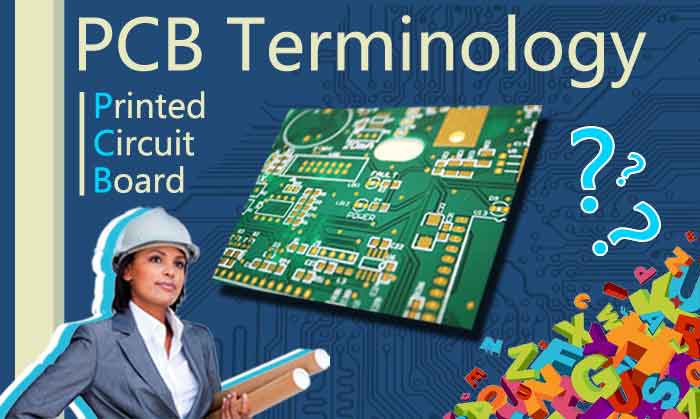
PCB Terminology Glossary (Beginners-Friendly) | PCB Design
"Are you confused with some printed circuit boards terminologies and looking for the pcb terminology definitions? In this page, we will bring you the most complete list of terminology in pcb design, yet some of them are the most common parts such as THM and SMT, but there are still a number of pcb manufacturing terminology you may not be aware of, this PCB terminology dictionary are sure to meet your need."
Sharing is Caring!
There are some basic recognitions of printed circuit board you need to know about, let's go through these questions before searching the PCB terminology!
1. What is a Printed Circuit Board?
A printed circuit board, or PCB, is used to mechanically support and electrically connect electronic components using conductive pathways, tracks or signal traces etched from copper sheets laminated onto a non-conductive substrate.
2. Who is Manufacturing High-Quality Printed Circuit Board?
FMUSER is the one of the most reliable PCB manufactuers around Asia, we know that any industry that uses electronic equipment requires PCBs. Whatever application you’re using your PCBs for, it’s important that they’re reliable, affordable, and designed to fit your needs.
As the expert in manufacturing PCBs of FM radio transmitter as well as the provider of audio and video transmission solutions, FMUSER also knows that you're looking for quality&budget PCBs for your FM broadcast transmitter, that's what we provide, contact us immediately for free PCB board inquiries!

3. What is Printed Circuit Board PCB Assembly?
Printed circuit board assembly is the process of connecting the electronic components with the wirings of printed circuit boards. The traces or conductive pathways engraved in the laminated copper sheets of PCBs are used within a non-conductive substrate in order to form the assembly
4. What is Printed Circuit Board PCB design?
Printed circuit board (PCB) design brings your electronic circuits to life in the physical form. Using layout software, the PCB design process combines component placement and routing to define electrical connectivity on a manufactured circuit board.
5. What Is the Importance of Printed Circuit Board?
The Printed Circuit Board (PCB) is very important in all electronic gadgets, which are used either for domestic use, or for industrial purpose. PCB design services are used to design the electronic circuits. Apart from electrically connecting, it also gives mechanical support to the electrical components.
6. How to Find PCB Terminology on Mobile Device / PC?
How do I Search PCB Terminology on Mobile Device?
Press the "Alphabet A - Alphabet Z" button from below for browsing the complete PCB terminology used in PCB design, PCB manufacturing and etc.
How do I Search PCB Terminology on PC?
● For precise PCB terminology searching, please press "Ctrl + F" buttons on your keyboard and type your word in.
● For viewing the whole PCB terminology list of a specific capitalized letter, please press "Alphabet A - Alphabet Z" button from below
Notice:
Printed Circuit Board Terminology Glossary (The First Letter Of Each Word Have Been Capitalized in order for better-searching)
We also prepare some interesting PCB posts for You:
What is Printed Circuit Board (PCB) | All You Need to Know
PCB Manufacturing Process | 16 Steps to Make a PCB Board
Through Hole vs Surface Mount | What is the Difference?
PCB Design | PCB Manufacturing Process Flow Chart, PPT, and PDF
How to Recycle A Waste Printed Circuit Board? | Things You Should Know
Let's begin browsing these PCB terminologies!
PCB Terminology Content (Click to Visit!):
Alphabet A, Alphabet B, Alphabet C, Alphabet D, Alphabet E, Alphabet F, Alphabet G, Alphabet H, Alphabet I, Alphabet J, Alphabet K, Alphabet L, Alphabet M, Alphabet N, Alphabet O, Alphabet P, Alphabet Q, Alphabet R, Alphabet S, Alphabet T, Alphabet U, Alphabet V, Alphabet W, Alphabet X, Alphabet Y, Alphabet Z
Printed Circuit Board Terminology Glossary PDF (Free Download)
Activating
A treatment that renders non-conductive material receptive to electroless deposition.Active component
A device that requires an external source of power to operate upon its input signal(s). Examples of active devices: transistors, rectifiers, diodes, amplifiers, oscillators, mechanical relays.
Additive Process
Deposition or addition of conductive material on clad or unclad base material.
AlN
Aluminum Nitride, a compound of aluminum with nitrogen.
AlN Substrate
A substrate of aluminum nitride.
Air gap
The minimum distance between features pad - pad, pad – traces and trace – trace
Alumina
A ceramic used for insulators in electron tubes or substrates in thin film circuits. It can withstand continuously with high temperatures and has a low dielectric loss over a wide frequency range. Aluminum oxide (Al2O3)
Ambient
The surrounding environment coming into contact with the system or component in question
Annular Ring: The width of the conductor pad surrounding a drilled hole. The pad area that remains after a hole is drilled through the pad. Designer tip: Try using teardrop shaped pads. They allow for any drill wander and / or Image shift during manufacturing and will help keep a healthy (over .002”) annular ring, at trace junction (required by IPC: A: 600).
Analog Circuit
An electrical circuit that provides a continuous quantitative output as a response from its input.
Aperture
An indexed shape with a specified x and y dimension, or line type with a specified width, used as a basic element or object by a photoplotter in plotting geometric patterns on film. The index of the aperture is its Position (a number used in an aperture list to identify an aperture) or D code.
Aperture wheel
A component of a vector photoplotter, it is a metal disk having cutouts with brackets and screw holes arranged near its rim for attaching apertures. Its center hole is attached to a motorized spindle on the lamp head of the photoplotter. When a D code denoting a particular position on the wheel is retrieved from a Gerber file by the photoplotter, the wheel is caused to rotate so that the aperture in that position is placed between the lamp and the film. In preparation for a photo plotting, the aperture wheel is set up by a technician who reads a printed aperture list, selects the correct aperture from a set of them stored in a box with compartments and, using a small screw driver, installs the aperture onto the position on the wheel which is called for on the list. This process is subject to human error and is one of the disadvantages of vector photoplotter as compared with laser photoplotter.
Aperture Information
This is a text file describing the size and shape of each element on the board. Also known as a D:code list. This report is not necessary if your files are saved as Extended Gerber with embedded Apertures (RS274X).
ApertureList/ApertureTable
A list of the shapes and sizes for describing the pads and tracks used to create a layer of a circuit board. Assembly File: A drawing describing the locations of components on a PCB.
AOI
(Automated Optical Inspection): Automatic laser/video inspection of traces and pads on the surface of inner layer cores or outer layer panels. The machine uses cam data to verify copper feature positioning, size and shape. Instrumental in locating "open" traces, missing features or "shorts".
AQL
(Acceptance Quality Level): The maximum number of defectives likely to exist within a population (lot) that can be considered to be contractually tolerable, normally associated with statistically derived sampling plans.
Array
A group of elements or circuits arranged in rows and columns on a base material.
Artwork Master
The photographic image of the PCB pattern on film used to produce the circuit board, usually on a 1:1 scale.
Aspect Ratio
T h e r a t i o o f t h e P C B t h i c k n e s s t o t h e d i a m e t e r o f t h e s m a l l e s t h o l e . The ratio of the board thickness to the smallest drilled hole. (Ex. 0.062” thick board 0.0135” drill = aspect ratio of 4.59:1). Designer tip: Minimizing the aspect ratio of the holes improves through hole plating and minimizes the chance of via failures
Artwork
Artwork for printed circuit design is photoplotted film (or merely the Gerber files used to drive the photoplotter), NC Drill file and documentation which are all used by a board house to manufacture a bare printed circuit board. See also Valuable Final Artwork.
ASCII
American Standard Code for Information Interchange. ASCII is the basis of character sets used in almost all present day computers.
Assembly
The process of positioning and soldering components to a PCB. 2. Act or process of fitting together parts to make a9+ whole.
Assembly drawing
A drawing depicting the locations of components, with their reference designators, on a printed circuit. Also called "component locator drawing."
Assembly house
A manufacturing facility for attaching and soldering components to a printed circuit.
ASTM
American Society of Testing and Materials.
AWG
American Wire Gauge. A PCB Designer needs to know diameters of wire gauges to properly size E pads. The American Wire Gauge, formerly known as the Brown and Sharp (B + S) Gauge, originated in the wire drawing industry. The gauge is calculated so that the next largest diameter always has a cross-sectional area that is 26% greater.
Automated Test Equipment (ATE)
Equipment that automatically test and analyzes functional parameters to evaluate performance of the tested electronic devices.
Automatic component placement
Machines are used to automate component placement. High-speed component placement machines, known as chip shooters, place the smaller, lower pin count components. More complex components with higher pin counts are placed by fine pitch machines that have greater precision.
Automatic optical component inspection
Post placement optical inspection of component presence/absence using automated systems.
Automatic X-Ray component/pin inspection
These inspection machines use X-Ray images to look under components are inside of the joints to determine the structural integrity of the solder connections.
Autorouter
Automatic router, a computer program that routes a PC board design (or a silicon chip design) automatically.
Array
A group of elements or circuits (or circuit boards) arranged in rows and columns on a base material.
▲BACK▲
BareBoard
A finished printed circuit board (PCB) that has no components mounted yet.It is also known as BBT.
BaseLaminate
The substrate material upon which the conductive pattern may be formed. The base material can be rigid or flexible.
Buriedvia
A via connects two or more inner layers but no outer layer, and cannot be seen from either side of the board.
Built in Self Test
An electrical testing method that allows the tested devices to test itself with specific added on hardware.
B:Stage
An intermediate stage in the reaction of a thermosetting resin in which the material softens when heated and swells, but does not entirely fuse or dissolve, when it is in contact with certain liquids.
Barrel
The cylinder formed by plating the walls of a drilled hole.
Base Material
The insulating material used to form the conductive pattern. It may be rigid or flexible or both. It may be a dielectric or insulated metal sheet.
Base Material Thickness
The thickness of the base material excluding metal foil or material deposited on the surface.
Bed of Nails
A test fixture consisting of a frame and a holder containing a field of spring loaded pins that make electrical contact with a planar test object.
Blister
A localized swelling and/or separation between any of the layers of a laminated base material, or between base material or conductive foil. It is a form of Delamination.
Board House
Board vendor. A manufacturer of printed circuit boards.
Board Thickness
The overall thickness of the base material and all conductive material deposited thereon. Almost any thickness of pcb can be produced, but 0.8mm, 1.6mm, 2.4, and 3.2mm are the commonest.
Book
A specified number of Prepreg plies which are assembled along with inner layer cores in preparation for curing in a lamination press.
Bond Strength
The force per unit area required to separate two adjacent layers of a board by a force perpendicular to the board surface.
Bow
The deviation from flatness of a board characterized by a roughly cylindrical or spherical curvature such that, if the product is rectangle, its four corners are in the same plane.
Border Area
The region of a base material that is external to that of the end product being fabricated within it.
Burr
A ridge surrounding the hole left on the outside copper surface after drilling.
Ball grid array - (Abbrev. BGA)
A flip chip type of package in which the internal die terminals form a grid style array, and are in contact with solder balls ( solder bumps ), which carry the electrical connection to the outside of the package. The PCB footprint will have round landing pads to which the solder balls will be soldered when the package and PCB are heated in a reflow oven. Advantages of the ball grid array package are (1) that its size is compact and (2) its leads do not get damaged in handling (unlike the formed "gull wing" leads of a QFP) and thus has a long shelf life. Disadvantages of the BGA are 1) they, or their solder joints, are subject to stress related failure. For example, the intense vibration of rocket powered space vehicles can pop them right off the PCB, 2) they cannot be hand soldered (they require a reflow oven), making first article prototypes a bit more expensive to stuff, 3) except for the outer rows, the solder joints cannot be visually inspected and 4) they are difficult to rework.
Base
The electrode of a transistor which controls the movements of electrons or holes by means of an electric field on it. It is the element which corresponds to the control grid of an electron tube.
Beam lead
A metal beam (flat metallic lead which extends from the edge of a chip much as wooden beams extend from a roof overhang) deposited directly onto the surface of the die as part of the wafer processing cycle in the fabrication of an integrated circuit. Upon separation of the individual die (normally by chemical etching instead of the conventional scribe:and:break technique), the cantilevered beam is left protruding from the edge of the chip and can be bonded directly to interconnecting pads on the circuit substrate without the need for individual wire interconnections. This method is an example of flip:chip bonding, contrasted with solder bump.
Board
Printed circuit board: A CAD database which represents the layout of a printed circuit.
Body
The portion of an electronic component exclusive of its pins or leads.
BOM[pronounced "bomb"]Bill of Materials
A list of components to be included on an assembly such as a printed circuit board. For a PCB the BOM must include reference designators for the components used and descriptions which uniquely identify each component. A BOM is used for ordering parts and, along with an assembly drawing, directing which parts go where when the board is stuffed.
Boundary Scan test
Edge connector test systems that utilize the IEEE 1149 standard for
describing test functionality that may be embedded within certain components.
Base Copper
The thin copper foil portion of a copper clad laminate for PCBs. It can be present on one or both sides of the board, and on inner layers.
Bevel
An angled edge of a printed board.
Blind Via
A conductive surface hole that connects an outer layer with an inner layer of a multilayer board.
B:Stage Material
Sheet material impregnated with a resin cured to an intermediate stage (B:stage resin). Prepreg is the popular term.
B:Stage Resin
A thermosetting resin that is in an intermediate state of cure.
Buildtime
The cutoff time for receiving orders and files is 2:00 pm (PST) Monday through Friday for Full Featured boards. Some files have been known to take 45 minutes to navigate the web, so please allow for this. Build time starts the following business day, unless a "hold" occurs.
▲BACK▲
CAD – (Computer Aided Design)
A system where engineers create a design and see the proposed product in front of them on a graphics screen or in the form of a computer printout or plot. In electronics, the result would be a printed circuit layout.
CAM – (Computer Aided Manufacturing)
The interactive use of computer systems, programs, and procedures in various phases of a manufacturing process wherein, the decision making activity rests with the human operator and a computer provides the data manipulation functions.
CAM Files
The data files used directly in the manufacture of printed wiring. The file types are: (1) Gerber files, which control a photoplotter. (2) NC Drill file, which controls an NC Drill machine. (3) Fabrication drawings in Gerber, HPGL or any other electronic format. Hard copy prints may be available also. CAM files represent the final product of PCB design. These files are given to the board house which further refines and manipulates CAM in their processes, for example in step and repeat panelization.
Chamfer
A broken corner to eliminate an otherwise sharp edge.
Card
Another name for a printed circuit board.
Capacitance
The property of a system of conductors and dielectrics that allows the storage of electricity when a potential difference exists between the conductors.
Catalyst
A chemical that is used to initiate the reaction or increase the speed of the reaction between a resin and a curing agent.
Ceramic Ball Grid Array (CBGA)
A ball grid array package with a ceramic substrate.
CEM1orCEM3
PCB board materials, standard epoxy resin with woven glass reinforcement over a paper core, differing only in the type of paper used. They are less expensive than Fr4.
Center to Center Spacing
The nominal distance between the centers of adjacent features on any single layer of a printed board, e.g.; gold fingers and surface mounts.
Check Plots
Pen plots, or plotted film, that are suitable for checking and for design approval by customers.
Chip on Board (COB)
A configuration in which a chip is directly attached to a printed circuit board or substrate by solder or conductive adhesives.
Check plots
Pen plots that are suitable for checking only. Pads are represented as circles and thick traces as rectangular outlines instead of filled in artwork. This technique is used to enhance transparency of multiple layers.
Chip
An integrated circuit manufactured on a semiconductor substrate and then cut or etched away from the silicon wafer. (Also called a die.) A chip is not ready for use until packaged and provided with external connections. Commonly used to mean a packaged semiconductor device.
Chip scale package
A chip package in which the total package size is no more than 20% greater than the size of the die within. Eg: Micro BGA.
Circuit
A number of electrical elements and devices that have been interconnected to perform a desired electrical function.
Circuit Board
A shortened version of PCB.
CIM (Computer Integrated Manufacturing)
Used by an assembly house, this software inputs assembly data from a PCB CAM/CAD package, such as Gerber and BOM, as input and, using a predefined factory modeling system, outputs routing of components to machine programming points and assembly and inspection documentation. In higher end systems, CIM can integrate multiple factories with customers and suppliers.
Circuitry Layer
A layer of a printed board containing conductors, including ground and voltage planes.
Clad
A copper object on a printed circuit board. Specifying certain text items for a board to be "in clad," means that the text should be made of copper, not silkscreen
Clearances
A clearance (or isolation) is a term we use to describe the space from power / ground layer copper to through hole. To prevent shorting, ground and power layer clearances need to be .025” larger than the finish hole size for the inner layers. This allows for registration, drilling, and plating tolerances.
Clearance Hole
A hole in the conductive pattern that is larger than, and coaxial with a hole in the base material of a printed board.
CNC (Computer Numerical Control)
A system that utilizes a computer and software as the primary numerical control technique.
Component
Any of the basic parts used in building electronic equipment, such as a resister, capacitor, DIP or connector, etc.
Component Hole
A hole that is used for the attachment and/or electrical connection of component terminations, including pins and wires, to a printed board.
ComponentSide
In order to prevent building a board inside out, we must be able to identify the correct orientation of your design. Component, layer 1, or 'top' layer should read in facing up. All other layers should line up as though looking through the board from the topside.
Conductive Pattern
The configuration pattern or design of the conductive material on a base material. (This includes conductors, lands, vias, heat sinks and passive components when those are integral parts of the printed board manufacturing process.
Conductor Spacing
The observable distance between adjacent edges (not center to center spacing) of isolated patterns in a conductor layer.
Continuity
An uninterrupted path for the flow of electrical current in a circuit.
Conformal Coating
An insulating & protective coating that conforms to the configuration of the object coated and is applied on the completed board assembly.
Connection
One leg of a net.
Connectivity
The intelligence inherent in PCB CAD software which maintains the correct connections between pins of components as defined by the schematic.
Connector
A plug or receptacle, which can be easily joined to or be separated from its mate. Multiple contact connectors join two or more conductors with others in one mechanical assembly.
Connector Area
The portion of the circuit board that is used for providing electrical connections.
Controlled Impedance
The matching of substrate material properties with trace dimensions and locations in an effort to create specific electric impedance for a signal moving along a trace. Conventional PCB: A rigid PCB with thickness 0.062” with wire leaded components, mounted only on one side of PCB, with all lead through hole soldered and clipped. Conventional circuitry is easier to debug and repair the surface mount.
Core Thickness
The thickness of the laminate base without copper.
Coating
A thin layer of material, conductive, magnetic or dielectric, deposited on a substance surface.
Coefficient of Thermal Expansion (CTE)
The ratio of dimensional change of an object to the original dimension when temperature changes, expressed in %/ºC or ppm/ºC.
Contact Angle (Wetting Angle)
The angle between the contact surfaces of two objects when bonding. The contact angle is determined by the physical and chemical properties of these two materials.
Copper Foil (Base Copper Weight)
Coated copper layer on the board. It can either be characterized by weight or thickness of the coated copper layer. For instance, 0.5, 1 and 2 ounces per square foot are equivalent to 18, 35 and 70 um:thick copper layers.
CopperFoil
Finished copper weight = 1oz.
Control Code
A non-printing character which is input or output to cause some special action rather than to appear as a part of data.
Core Thickness
The thickness of the laminate base without copper.
Corrosive Flux
A flux that contains corrosive chemicals such as halides, amines, inorganic or organic acids that can cause oxidation of copper or tin conductors.
Crosshatching
The breaking up of large conductive area by the use of a pattern of voids in the conductive material.
Curing
The irreversible process of polymerizing a thermosetting epoxy in a temperature time profile.
Curing Time
The time needed to complete curing of an epoxy at a certain temperature.
Cutlines
A cut line is what our system uses to program the router specifications. It represents the outer dimensions of your board. This is required for the board to finish as the size you want it.
▲BACK▲
Alphabet D
Database
A collection of interrelated data items stored together without unnecessary redundancy, to serve one or more applications.
Date Code
Marking of products to indicate their date of manufacture. ACI standard is WWYY (weekweekyearyear).
Datum
The theoretically: exact point, axis or plane that is the origin from which the location of geometric characteristics of features of a part are established.
Delamination
A separation between plies within a base material, between a base material and a conductive foil, or any other planner separation with a printed board.
Design Rule Checking
The use of a computer: aided program to perform continuity verification of all conductors routing in accordance with appropriate design rules.
Desmear
The removal of friction melted resin and drilling debris from a hole wall.
Destructive testing: Sectioning a portion of printed circuit panel and examining the sections with a microscope. This is performed on coupons, not the funtional part of the PCB.
Dewetting
A condition that results when molten solder has coated a surface and then receded. It leaves irregularly shaped mounds separated by areas of thin solder. The base material is not exposed.
DFSM
Dry Film Solder Mask.
Die
Integrated circuit chip as diced or cut from a finished wafer.
Die Bonder
The placement machine bonding IC chips onto a chip on board substrate.
Die Bonding
The attachment of an IC chip to a substrate.
Dimensional Stability
A measure of the dimensional change of a material that is caused by factors such as temperature changes, humidity changes, chemical treatment, and stress exposure.
Dimensioned Hole
A hole in a printed board whose location is determined by physical dimensions or coordinate values that do not necessarily coincide with the stated grid.
DoubleSidePCB
The PCB having two circuit layers with pads & traces are on both sides of the board.
Double sided Laminate: A bare PCB laminate having tracks on both sides, normally PTH holes connecting circuitry two sides together.
Double side component assembly
Mounting component on both sides of PCB, for e.g. SMD technology.
DrillToolDescription
This is a text file describing drill tool number and corresponding size. Some reports also include quantity. Please Note: All drill sizes will be interpreted as plated through finished sizes unless otherwise specified.
DrillFile
In order to process your order, we require a drill file (with x:y coordinates) that is viewable in any text editor.
Dry Film Resists
Coated photosensitive film on the copper foil of PCB using photographic methods. They are resistant to electroplating and etching processes in the manufacturing process of PCB.
Dry Film Solder Mask
A solder mask film applied to a printed board using photographic methods. This method can manage the higher resolution required for fine line design and surface mount.
▲BACK▲
A connector on the circuit board edge in the form of gold plated pads or lines of coated holes used to connect other circuit board or electronic device.
Edge Clearance
The smallest distance from any conductors or components to the edge of the PCB.
Electrode deposition
The deposition of a conductive material from a plating solution by the application of electrical current.
Electroless Desposition/Plating
The deposition of conductive material from an auto catalytic reduction of a metal ion on certain catalytic surfaces.
Electroplating
The electrode position of a metal coating on a conductive object. The object to be plated is placed in an electrolyte and connected to one terminal of a DC voltage source. The metal to be deposited is similarly immersed and connected to the other terminal. Ions of the metal provide transfer to metal as they make up the current flow between the electrodes.
Electrical Test
(1-sided / 2-sided) Testing is used primarily to test for opens and shorts. PCBpro recommends testing for all surface mount boards and multi-layer orders (3 layers & up). The quoted price is accurate up to 1000 test points for a one-sided test fixture, and up to 600 points for a double-sided surface mount test fixture.
A version of CAD,CAM and CAE in which the software packages used and their inputs and outputs are integrated with each other and allow design to flow smoothly with no manual intervention necessary (other than a few keystrokes or menu selections) to get from one step to the other. Flow can occur in both directions. In the field of PCB design, end-to-end design sometimes refers to only the electronic schematic/pcb layout interface, but this is a narrow view of the potentialities of the concept
E-pad
“Engineering-pad." A plated-through hole or surface mount pad on a PCB placed on the board for the purpose of attaching a wire by soldering. These are usually labeled with silkscreen. E-pads are used to facilitate proto-typing, or simply because wires are used for interconnections instead of headers or terminal blocks.
Epoxy
A family of thermosetting resins. Epoxies form a chemical bond to many metal surfaces.
Epoxy Smear
Epoxy resin that has been deposited on edges of copper in holes during drilling either as uniform coating or in scattered patches. It is undesirable because it can electrically isolate the conductive layers from the plated-through-hole interconnections.
ESR
Electro-statically applied Solder Resist.
Etching
Removing unwanted metallic substance by chemical or chemical/electrolytic process
Etch back
The controlled removal by a chemical process, to a specific depth, of nonmetallic materials from the sidewalls of holes in order to remove resin smear and to expose additional internal conductor surfaces.
Excellon Drill File
In order to process your order, we require a drill file (with x-y coordinates) that is viewable in any text editor.
▲BACK▲
FR-1
A paper material with a phenolic resin binder. FR-1 has a TG of about 130°C.
FR-2
A paper material with phenolic resin binder similar to FR-1 - but with a TG of about 105°C.
FR-3
A paper material that is similar to FR-2 - except that an epoxy resin is used instead of phenolic resin as a binder. Used mainly in Europe.
FR-4
The most commonly used PCB board material. "FR" stands for Flame Retardant and "4" means woven glass reinforced epoxy resin.
FR-6
Fire-Retardant glass-and-polyester substrate material for electronic circuits. Inexpensive; popular for automobile electronics
Functional Test
The electrical testing of an assembled electronic device with simulated function generated by the test hardware and software.
▲BACK▲
Gerber Files
Industry standard format for files used to generate artwork necessary for circuit board imaging. The preferred Gerber format is RS274X, which embeds the apertures within the specific files. The apertures assign specific values to design data (specific pad size, trace width, etc.), and these values make up a D-code list. When files are not saved as RS274X, a text file with values must be included because the values must be hand-entered by our CAM operators. This slows down the process and increases the margin for human error, as well as lead-time and cost.
A laminate consisting of woven epoxy-glass cloth impregnated with epoxy resin under pressure and heat. G10 lacks the anti-flammability properties of FR-4. Used mainly for thin circuits such as in watches.
Gerber CAM Viewer
There are many Gerber viewers in the market. Here is a short list: GC Prevue, View Mate, GerbTool, CAM 350, CAMTASTIC, CAMCAD, CAM Expert, Evgraver, View Plot etc.
Gerber Viewer Recommendations – View mate :Use the parameters on our pcb capabilities page to
learn about our manufacturing capabilities prior to layout of your design, and prevent processing failures. By setting the pad sizes, clearances, minimum traces and spaces so your design will make it through the manufacturing process and will prevent board failures.
GI
The woven glass fiber laminate impregnated with polyimide resin.
Glob top
A blob of non-conductive plastic, often black in color, which protects the chip and wire bonds on a packaged IC and also on a chip on board . This specialized plastic has a low coefficient of thermal expansion so that ambient temperature changes will not rip loose the wire bonds it is designed to protect. In high-volume chip on board production, these are deposited by automated machinery and are round. In prototype work, they are deposited by hand and can be custom-shaped; however, in designing for manufacturability, one assumes a prototype product will "take- off" and ultimately have high market demand, and so lays out chip on board to accommodate a round glob top with adequate tolerance for machine-driven "slop-over".
Glue deposit
Glue is automatically placed at the center of a component for extra structural integrity as a bonding agent between the component and the board.
Gold Finger
The gold-plated terminal of a card-edge connector.
▲BACK▲
NONE
Interconnect Stress Test
The IST system is designed to quantify the ability of the total interconnect to withstand the thermal and mechanical strains, from the as manufactured state, until the product reaches the point of interconnect failure.
Interstitial Via Hole
An embedded through-hole with connection of two or more conductor layers in a multilayer PCB.
Immersion coating
Electroless coating of copper in traditional pcb manufacture to achieve the basis of through hole plating, and/or the electroless deposition of tin, silver, or nickel and gold to pads and holes to offer a solderable finish to the circuitry. Tracks might also be coated in this way for particular reasons.
IPC–(The Institute for Interconnecting and Packaging Electronic Circuits)
The final American authority on how to design and manufacture printed Circuit Board.
▲BACK▲
NONE
A board or assembly that is verified to be free of defects. Also known as a Golden Board.
▲BACK▲
A composite material made by bonding together several layers of same or different materials.
Lamination
The process of manufacturing a laminate using pressure and heat.
Laminate Thickness
Thickness of the metal-clad base material, single or double-sided, prior to any subsequent processing.
Laminate Void
An absence of epoxy resin in any cross-sectional area that should normally contain epoxy resin.
Land
The portion of the conductive pattern on printed circuits designated for the mounting or attachment of components. Also called a pad.
Laser Photo-Plotter
A plotter that uses a laser, which simulates a vector photo-plotter by using software to create a raster image of the individual objects in a CAD database, then plots the image as a series of lines of dots at a very fine resolution. A laser photo-plotter is capable of more accurate and consistent plots than a vector plotter.
Layer Sequence
Layer sequence helps to build the layer stack up from top to bottom and one can and its very help to CAD to identify the type of layer.
Layers
The layers give indication of different sides of PCB. On-board text such as company name, logo, or part number that is oriented right-reading on the top layer will quickly allow us to determine that files have been imported correctly. This simple step can save a time-consuming hold notice and potential hold up. Please note: any traces on outer layer that are 0.010" wide or less will require ½ ounce copper starting weight to prevent excessive trace width reduction.
Lay up
The process in which treated prepegs and copper foils are assembled for pressing.
Leakage Current
A small amount of current that flows across a dielectric area between two adjacent conductors.
Legend
A format of printed letters or symbols on the PCB, such as part numbers and product number or logos.
Lot
A quantity of circuit board that share a common design.
Lot Code
Some Customers require a manufacturer's lot code to be placed on the board for future tracking purposes. A drawing can specify the location, what layer and if it is to be in copper, mask opening, or silkscreen. This option is available on the Full-Featured instant quote.
LPI – (Liquid Photo-Imageable Solder Mask)
An ink that is developed off using photographic imaging techniques to control deposition. It is the most accurate method of mask application and results in a thinner mask than dry film solder mask. It is often preferred for dense SMT. Application can be spray or curtain coat.
▲BACK▲
Major Defect
A defect that is likely to result in failure of a unit or product by materially reducing its usability for its intended purpose.
Mask
A material applied to enable selective etching, plating, or the application of solder to a PCB. Also called solder mask or resist.
Master aperture list
Any aperture list which is used for two or more PCB’s is called master aperture list for that set of PCB.
Measling
Discrete white spots or crosses below the surface of the base laminate that reflect a separation of fibers in the glass cloth at the weave intersection.
Metal Foil
The plane of conductive material of a printed board from which circuits are formed. Metal foil is generally copper and is provided in sheets or rolls.
Micro-Sectioning
The preparation of a specimen of a material, or materials, used in metallographic examination. This usually consists of cutting out a cross-section followed by encapsulation, polishing, etching, and staining.
Microvia
Usually defined as a conductive hole with a diameter of 0.005" or less that connects layers of a multi- layer PCB. Often used to refer to any small geometry connection holes created by laser drilling.
Mil
One thousandth of an inch.
Minimum Traces & Spacing
Traces are the “Wires” of the Printed Circuit Board (also known as tracks). Spaces are the distances between traces, the distances between pads, or the distances between a pad and a trace. How wide is the smallest trace (line, track, wire), or space between traces or pads? Whichever is less of the two governs the order form selection.
Mounting Hole
A hole that is used for the mechanical support of a printed board or for the mechanical attachment of components to a printed board.
Minimum Conductor Width
The smallest width of any conductors, such as traces, on a PCB.
Minimum Conductor Space
The smallest distance between any two adjacent conductors, such as traces, in a PCB.
Minor Defect
A defect that is not likely to result in the failure of a unit of product or that does not reduce the usability for its intended purpose.
Multilayer PCB
The pads and traces are on both sides and also there are traces embedded within the board. Such PCB’s are called Multilayer PCB.
▲BACK▲
NC Drill
Numeric Control drill machine used to drill holes at exact locations of a PCB specified in NC Drill File.
NC drill file
A text file which tells an NC drill where to drill its holes.
Negative
A reverse-image copy of a positive, useful for checking revisions of a PCB and is often used for representing inner layer planes. When a negative image is used for an inner-layer it would typically have clearances (solid circles) and thermals (segmented donuts) that either isolate holes from the plane or make thermally relieved connections respectively.
Net
A collection of terminals all of which are, or must be, connected electrically. Also known as signal.
Netlist
List of names of symbols or parts and their connection points which are logically connected in each net of a circuit. A netlist can be captured from properly prepared schematic-drawing files of an electrical CAE application.
Node
A pin or lead to which at least two components are connected through conductors.
Notation
A diagram on PCB to indicate the orientation and location of components.
Nomenclature
Identification symbols applied to the board by means of screen printing, inkjetting, or laser processes.
Notch
It is also called a slot, it can be seen only on the external side of the board, generally seen in mechanical layers used for routing.
Non-plated Through Hole. We recommend that you include a drill drawing to identify the non-plated holes in your design. Because design packages often calculate the amount of clearance around a non- plated hole differently than a plated hole, the non-plated holes can end up with less allowance for passing through solid copper ground and power planes. While this is not a problem when the non- plated information is supplied in a drill drawing, it only becomes one if the non-plated information is omitted. The result being mounting holes that short the power and ground planes together. Remember to always identify your non-plated holes.
Number of Holes
This is the total number of holes in the board. There is no influence on price and no limit to quantity of holes on PCB.
▲BACK▲
Open
Open circuit. An unwanted break in the continuity of an electrical circuit which prevents current from flowing.
OSP
Organic solder preservative also known as Organic Surface Protection is the lead-free procedure and meets the full requirements of the RoHS-Compliance.
Outer-Layer
The top and bottom sides of any type of circuit board.
▲BACK▲
Pad
The portion of the conductive pattern on printed circuits designated for the mounting or attachment of components.Pad annulus
Typically refers to the width of the ring of metal around a hole in a pad.
Part Number
The name or number associated with your printed circuit board for your convenience.
Panel
A rectangular sheet of base material or metal-clad material of predetermined size that is used for the processing of printed boards and, when required, one or more test coupons.
Pattern
The configuration of conductive and nonconductive materials on a panel or printed board. Also, the circuit configuration on related tools, drawing, and masters.
Pattern Plating
The selective plating of a conductive pattern.
PCB
Printed Circuit Board. Also called Printed Wiring Board (PWB).
PCB database
All of the data fundamental to a PCB design , stored as one or more files on a computer.
PCB-Design-Software/Tools
Software that helps designer to do schematic, layout design, routing and optimizations, etc. There are many design software and tools in the market. Some of them are free PCB design software. Here is a short list: ExpressPCB, EAGLE, PROTEL, CADSTAR, ORCAD, CIRCUIT MAKER, P-CAD 2000, PCB ELEGANCE, EDWIN, VISUALPC, BPECS32, AUTOENGINEER, EXPERT PCB, CIRCAD, LAYOUT, CIRCUIT LAYOUT, MCCAD, DREAM CAD, E-CAD, POWERPCB, PCB ASSISTANT, PCB DESIGNER, QCAD, QUICK ROUTE, TARGET 3001, WIN CIRCUIT 98, BOARD EDITOR, PCB, VUTRAX, CIRCUIT CREATOR, PADSPCB, DESIGN WORKS, OSMOND PPC, LAY01, SCORE, GElectronic, PRO-Board, PRO-Net , CSIEDA, VISUALPCB, WINBOARD, ULTIBOARD, EASY PC, RANGER, PROTEUS, EPD -Electronics Packaging Designer , AutoTrax Eda, Sprint Layout, CADINT, KICAD, Merlin PCB Designer,
FREE-PCB, TinyCAD, WINQCAD, Pulsonix, DIPTRACE.
A general process can be simplified as: Copper laminate -> Drill board -> Deposit Cu -> Photolithography -> Tin lead plate or finishing -> Etch -> Hot air level -> Solder mask -> E-Testing -
> Routing/V-scoring -> Product inspection -> Final cleanning -> Packaging . (Note : Procedure is
same for manufacturing but varies with respect to different manufacturer)
Personal Computer Memory Card International Association.
PEC
Printed Electronic Component.
Phenolic PCB
It is cheaper laminate material different from fibre glass material.
Photographic Image
An image in a photo mask or in an emulsion that is on a film or plate.
Photo Print
The process of forming a circuit pattern image by hardening a photosensitive polymeric material by passing light through a photographic film.
Photo-Plotting
A photographic process whereby an image is generated by a controlled light beam that directly exposes a light-sensitive material.
Photo-Resist
A material that is sensitive to portions of the light spectrum and that, when properly exposed can mask portions of a base metal with a high degree of integrity.
Photo-tool
A transparent film that contains the circuit pattern, which is represented by a series of lines of dots at a high resolution.
Pin
A terminal on a component, whether SMT or through-hole. Also called a lead.
Pitch
The center-to-center spacing between conductors, such as pads and pins, on a PCB.
A manufacturing operation of assembly process in which components are selected and placed onto specific locations according to the assembly file of the circuit.
PTH
Plated Through Hole, a hole with the plated copper on its sides to provide electrical connections between conductive patterns at the levels of a printed circuit board. There are two types of PTH. One is for mounting components and the other is not used to mount component.
Plating
The chemical or electrochemical process in which metal is deposited on a surface.
The area of absence of a specific metal from a specific cross-sectional area.
A component package with J-leads.
Plating Resist
Material deposited as a covering film on an area to prevent plating on this area.
Plots
The masters for photo-tools produced from Gerber files.
Positive
Developed images of photo-plotted file, where the areas selectively exposed by the photo-plotter appear black and unexposed areas are clear. For outer-layers, color will indicate copper. Positive inner-layers will have clear areas to indicate copper.
Prepreg
A sheet of material that has been impregnated with a resin cured to an intermediate stage. I.e. B-stage resin.
Platen
A flat plate of metal within the lamination press in between in which stacks are placed during pressing.
Prototype
A pcb made and built to test a design.
▲BACK▲
Quantity
This is used to generate the information in the Price Matrix price table.
QFP
Quad Flat Pack, a fine-pitch SMT package that is rectangular or square with gull-wing shaped leads on all four sides
Ratsnest
A bunch of straight lines (unrouted connections) between pins which represents graphically the connectivity of a PCB CAD database.
The name of components on a printed circuit by convention beginning with one or two letters followed by a numeric value. The letter designates the class of component; e.g. "Q" is commonly used as a prefix for transistors. Reference designators appear as usually white or yellow epoxy ink (the "silkscreen") on a circuit board. They are placed close to their respective components but not underneath them. So that they are visible on the assembled board.
A dimension without a tolerance that is used only for informational purposes that does not govern inspection or other manufacturing operations.
Registration
The degree of conformity to the position of a pattern, or a portion thereof, a hole or other feature to its intended position on a product.
Readme File
A text file included in the zip file, which provides necessary information needed to manufacture your order. Phone numbers or email addresses of designer or engineer contacts for this project should be included to expedite resolution of any potential manufacturing problems that could delay your order.
Reflow oven
Boards pass through an oven in which the solder paste was deposited earlier.
Reflow Soldering
Melting, joining and solidification of two coated metal layers by application of heat to the surface and predeposited solder paste.
Resist
Coating material used to mask or to protect selected areas of a pattern from the action of an etchant, solder, or plating.
Resin (Epoxy) Smear
Resin transferred from the base material onto the surface of the conductive pattern in the wall of a drilled hole.
Rigid-flex
A PCB construction combining flexible circuits and rigid multi-layers usually to provide a built-in connection or to make a three-dimension form that includes components.
Revision
If you have the same drawing number but updated revisions, please enter it here. This will avoid any confusion for manufacturing your desired boards. Please make sure that your revision number is included with your drawings.
RF (radio frequency) and wireless design
A circuit design that operates in a range of electromagnetic frequencies above the audio range and below visible light. All broadcast transmission, from AM radio to satellites, falls into this range, which is between 30KHz and 300GHz.
RoHS
Restriction of Hazardous Substances is one of a handful of European legislation intended to eliminate or severely curtail the use of cadmium, hexavalent chromium, and lead in all products from automobiles to consumer electronics.
RoHS Compliant PCB
PCB boards that are processed under RoHS regulations. Route (or Track): A layout or wiring of an electrical connection.
Router
A machine that cuts away portions of the laminate to form the desired shape and size of the printed board.
▲BACK▲
Schematic
A diagram which shows, by means of graphic symbols, the electrical connections and functions of a specific circuit arrangement.
Scoring
A technique in which grooves are machined on opposite sides of a panel to a depth that permits individual boards to be separated from the panel after component assembly.
Screen Printing
A process for transferring an image from a patterned screen to a substrate through a paste forced by a squeegee of a screen printer.
Short: Short circuit
An abnormal connection of relatively low resistance between two points of a circuit. The result is excess (often damaging) current between these points. Such a connection is considered to have occurred in a printed wiring CAD database or artwork anytime conductors from different nets either touch or come closer than the minimum spacing allowed for the design rules being used.
Short run
Depends on the size of the manufacturing facility and the size of the printed circuit boards to be made. A short manufacturing run of printed circuits means from one to tens of panels of pcbs required to fulfill the order rather than hundreds.
Silk Screen (Silk Legend)
Epoxy-ink Legend printed on PCB. The most common colors used are white and yellow.
Sieber Meyer
In order to process your order, we require a drill file (with x:y coordinates) that is viewable in any text editor
Single Side PCB
The pads and traces are on the one side of the board only.
Single track
PCB design with only one route between adjacent DIP pins.
Small Outline Integrated Circuit (SOIC)
An integrated circuit with two parallel rows of pins in surface mount package.
All dimensions are in inches or metric. If board is in metric, please convert to inches. Please note, maximum X & Y configuration 108" This means if the width (X) is 14", then the maximum length (Y) is 7.71".
SMOBC
Solder mask over bare copper.
SMD
Surface Mount Device.
SMT
Surface Mount Technology.
Solder Bridging
Solder connecting, in most cases, misconnecting, two or more adjacent pads that come into contact to form a conductive path.
Solder Bumps
Round solder balls bonded to the pads of components used in face-down bonding techniques.
Solder Coat
A layer of solder that is applied directly from a molten solder bath to a conductive pattern.
Solder Leveling
The process by which the board is exposed to hot oil or hot air to remove excess solder from holes and lands.
Solder Mask or Solder resist
Coating to prevent solder to deposit on.
Solder Mask
Used to protect the board and circuitry during the assembly and packaging operations. Among other things, the solder mask helps prevents solder bridges between adjacent pads and traces during the wave soldering process.
Solder Mask (Artwork)
To generate your Soldermask artwork, add your smallest space measurement to the pad size. For boards with 0.006" spaces, use a pad size up to +0.006" up to 0.010" for 0.010". Spaces larger than 0.010" should have a pad size of +0.010".
Please note
While we make every attempt to leave a mask "dam" between surface mounts, fine pitch areas will be relieved in strips. Our manufacturing process needs at least 0.005" mask "dam" between pads in order to adhere to the board. Pad-to-pad spacing less than 0.013" may not have solder mask between them.
SolderMaskColor
There are different types of colour used for solder mask, for e,g Green, Red, Blue and white etc..
Solder paste
Associated with SMT. A paste screened onto a pcb or panel of pcbs to facilitate the placing and soldering of surface mount components. Also used to refer to the Gerber file used to produce the stencil/screen.
Solder Wick
A band of wire removes molten solder away from a solder joining or a solder bridge or just for desoldering.
SPC
Statistical Process Control. The collection of process data and creation of control charting is a tool used to monitor processes and to assure that they remain in control or stable. Control charts help distinguish process variation due to assignable causes from those due to unassignable causes.
Step-and-Repeat
The successive exposure of a single image on order to produce a multiple-image production master. Also used in CNC programs.
Stuff
Components are attached and soldered to a printed circuit board. Often done by an assembly house.
Sub-Panel
A group of printed circuits arrayed in a panel and handled by both the board house and the assembly house as though it were a single printed wiring board. The sub-panel is usually prepared at the board house by routing most of the material separating individual modules leaving small tabs.
Substrate
A material on whose surface adhesive substance is spread for bonding or coating. Also, any material that provides a supporting surface for other materials used to support printed circuit patterns.
Surface Mount
The pitch of the surface mount is defined as the dimension in inches from center to center of surface mount pads. Standard pitch is >0.025", fine pitch is 0.011"-0.025", and ultra fine pitch is <0.011". As boards contain finer pitch, processing and test fixture costs increase.
Surface finish
It is the type of finish required by customer for his board. The different surface finishing processes are HASL, OSP, Immersion gold, Immersion silver, Gold plating for all of regular boards.
▲BACK▲
Tape Automated Bonding
Tab Routing (with & without perforation holes)
Rather that completing the route path around the board edge, “Tabs” are left so as to leave boards attached in pallets for ease in assembly. And it also provides good mechanical strength to the board.
Temperature Coefficient (TC)
The ratio of a quantity change of an electrical parameter, such as resistance or capacitance, of an electronic component to the original value when temperature changes, expressed in %/ºC or ppm/ºC.
Tented Via
A via with dry film solder mask completely covering both its pad and its plated-thru hole. This completely insulates the via from foreign objects, thus protecting against accidental shorts, but it also renders the via unusable as a test point. Sometimes vias are tented on the topside of the board and left uncovered on the bottom side to permit probing from that side only with a text fixture.
Tenting
The covering of holes in a printed board and the surrounding conductive pattern with a dry film resist.
Terminal
A point of connection for two or more conductors in an electrical circuit; one of the conductors is usually an electrical contact or lead of a component.
Test Board
A printed board that is deemed to be suitable for determining the acceptability of a group of boards that were. Or will be, produced with the same fabrication process.
Test Fixture
A device that interfaces between test equipment and the unit under test.
Test Point
A specific point in a circuit board used for specific testing for functional adjustment or quality test in the circuit-based device.
Testing
A method for determining whether sub-assemblies, assemblies and/or a finished product conform to a set of parameter and functional specifications. Test types include: in-circuit, functional, system- level, reliability, environmental.
Test Coupon
A portion of a printed board or of a panel containing printed coupons used to determine the acceptability of such a board.
TG (Tg)
Glass transition temperature. The point at which rising temperatures cause resin inside the solid base laminate to start to exhibit soft, plastic-like symptoms. This is expressed in degrees Celsius (°C).
Thief
An extra cathode placed as to divert to itself some of the current from portions of the board which otherwise would receive too high a current density.
Through-Hole
Having pins designed to be inserted into holes and soldered to pads on a printed board. Also spelled "thru-hole".
Tooling
The processes and/or costs of setting up to manufacture a run of pcbs for the first time. .
Tooling Holes
The general term for holes placed on a PCB or a panel of PCBs for registration and hold-down purposes during the manufacturing process.
Trace/Track
Segment of a conductor route or net.
Traveler
The list of instructions describing the board, including any specific processing requirements. Also called a shop traveler, routing sheet, job order, or production order.
Turnkey
A type of outsourcing method that turns over to the subcontractor all aspects of manufacturing including material acquisition, assembly and testing. Its opposite is consignment, where the outsourcing company provides all materials required for the products and the subcontractor provides only assembly equipment and labour.
Twist
A laminate defect in which deviation from planarity results in a twisted arc.
▲BACK▲
UL: (Underwriters Laboratories Inc.)
A corporation supported by some underwriters for the purpose of establishing safety standards on types of equipment or components.
Underwriters Symbol
A logotype denoting that a product has been recognized (accepted) by Underwriters Laboratories Inc. (UL).
Unclad
Cured Epoxy glass without any copper layer(s).
UV Curing
Polymerizing, hardening, or cross linking a low molecular weight resinous material in a wet coating ink using ultra violet light as an energy source.
▲BACK▲
Valuable Final Artwork
A term used in "Streamlined PCB Design“.Artwork for electronic circuits which have been laid out and documented in forms, perfectly suited to the photo-imaging and numeric-controlled tooling processes of printed circuit manufacture. It is termed "final" because it has been thoroughly checked for errors and any corrected as needed and is now ready for manufacture without further work by the PCB designer . It is valuable because it could be exchanged with a customer for money or other support.
Via
A plated through hole (PTH) in a Printed Circuit Board that is used to provide electrical connection between a trace on one layer of the Printed Circuit Board to a trace on another layer. Since it is not used to mount component leads, it is generally a small hole and pad diameter.
Void
The absence of any substances in a localized area. (e.g. missing plating in a hole, or missing track).
V-Scoring
Rather than completing a route path around the board edge, the edges are "scored" to allow breaking boards apart after assembly. This is another way to palletize / panelized the boards. This method creates two beveled scoring lines along the perimeter of your boards. This makes it easier to break apart the boards at a later date. You would receive your boards in panel form like tab routing.
▲BACK▲
Alphabet - W
Wave Soldering
A process in which assembled printed boards are brought in contact with a continuously flowing and circulating mass of solder, typically in a bath to connect the leads of components to through hole pads and barrels, is called wave soldering.
Wet solder mask
A wet solder mask is a distribution of wet epoxy ink through a silk screen, has a resolution suitable for single-track design, but is not accurate enough for fine-line design.
Wicking
Migration of copper salts into the glass fibers of the insulating material found in the barrel of a plated hole.
Wire
Besides its usual definition of a strand of conductor, wire on a printed board also means a route or track.
Wire wrap area
A portion of a board riddled with plated-through holes on a 100-mil grid. Its purpose is for accepting circuits which may be found necessary after a PCB has been manufactured, stuffed, tested and debugged.
▲BACK▲
X-Axis
The horizontal or left-to-right direction in a two-dimensional system of coordinates.
Y-Axis
The vertical or bottom-to-top direction in a two-dimensional system of coordinates.
Alphabet - Z
Zip File
All files needed for the processing of your order must be compressed in a zip file. Due to the large amount of orders received. WinZip or Pkzip can be downloaded from pcb links page.
Z-Axis
The axis perpendicular to the plane formed by the X and Y datum reference. This axis usually represents the thickness of the boards.
FMUSER knows that any industry that uses electronic equipment requires PCBs. Whatever application you’re using your PCBs for, it’s important that they’re reliable, affordable, and designed to fit your needs.
As the expert in manufacturing PCBs of FM radio transmitter as well as the provider of audio and video transmission solutions, FMUSER also knows that you're looking for quality&budget PCBs for your FM broadcast transmitter, that's what we provide, contact us immediately for free PCB board inquiries!
Like it? Share it!
▲BACK▲