
Products Category
- FM Transmitter
- 0-50w 50w-1000w 2kw-10kw 10kw+
- TV Transmitter
- 0-50w 50-1kw 2kw-10kw
- FM Antenna
- TV Antenna
- Antenna Accessory
- Cable Connector Power Splitter Dummy Load
- RF Transistor
- Power Supply
- Audio Equipments
- DTV Front End Equipment
- Link System
- STL system Microwave Link system
- FM Radio
- Power Meter
- Other Products
- Special for Coronavirus
Products Tags
Fmuser Sites
- es.fmuser.net
- it.fmuser.net
- fr.fmuser.net
- de.fmuser.net
- af.fmuser.net ->Afrikaans
- sq.fmuser.net ->Albanian
- ar.fmuser.net ->Arabic
- hy.fmuser.net ->Armenian
- az.fmuser.net ->Azerbaijani
- eu.fmuser.net ->Basque
- be.fmuser.net ->Belarusian
- bg.fmuser.net ->Bulgarian
- ca.fmuser.net ->Catalan
- zh-CN.fmuser.net ->Chinese (Simplified)
- zh-TW.fmuser.net ->Chinese (Traditional)
- hr.fmuser.net ->Croatian
- cs.fmuser.net ->Czech
- da.fmuser.net ->Danish
- nl.fmuser.net ->Dutch
- et.fmuser.net ->Estonian
- tl.fmuser.net ->Filipino
- fi.fmuser.net ->Finnish
- fr.fmuser.net ->French
- gl.fmuser.net ->Galician
- ka.fmuser.net ->Georgian
- de.fmuser.net ->German
- el.fmuser.net ->Greek
- ht.fmuser.net ->Haitian Creole
- iw.fmuser.net ->Hebrew
- hi.fmuser.net ->Hindi
- hu.fmuser.net ->Hungarian
- is.fmuser.net ->Icelandic
- id.fmuser.net ->Indonesian
- ga.fmuser.net ->Irish
- it.fmuser.net ->Italian
- ja.fmuser.net ->Japanese
- ko.fmuser.net ->Korean
- lv.fmuser.net ->Latvian
- lt.fmuser.net ->Lithuanian
- mk.fmuser.net ->Macedonian
- ms.fmuser.net ->Malay
- mt.fmuser.net ->Maltese
- no.fmuser.net ->Norwegian
- fa.fmuser.net ->Persian
- pl.fmuser.net ->Polish
- pt.fmuser.net ->Portuguese
- ro.fmuser.net ->Romanian
- ru.fmuser.net ->Russian
- sr.fmuser.net ->Serbian
- sk.fmuser.net ->Slovak
- sl.fmuser.net ->Slovenian
- es.fmuser.net ->Spanish
- sw.fmuser.net ->Swahili
- sv.fmuser.net ->Swedish
- th.fmuser.net ->Thai
- tr.fmuser.net ->Turkish
- uk.fmuser.net ->Ukrainian
- ur.fmuser.net ->Urdu
- vi.fmuser.net ->Vietnamese
- cy.fmuser.net ->Welsh
- yi.fmuser.net ->Yiddish
What is Printed Circuit Board (PCB) | All You Need to Know
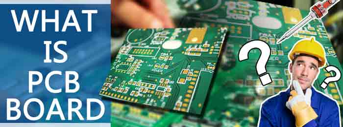
"PCB, also known as a printed circuit board, is made of different sheets of a non-conductive material, is used to physically support and connect the surface-mounted socketed components. But, what are the functions of a PCB board? Read the following content for more useful info! ---- FMUSER"
Are you looking for answers to the following questions:
What does a printed circuit board do?
What is a printed circuit called?
What is a printed circuit board made of?
How much is a printed circuit board?
Are printed circuit board toxic?
Why is it called a printed circuit board?
Can you throw away circuit boards?
What are the parts of a circuit board?
How much does it cost to replace a circuit board?
How do you identify a circuit board?
How does a circuit board work?
Or, maybe you're not so sure whether you know the answers to these questions, but please don't worry, as an expert in electronics and RF engineering, FMUSER will introduce all you need to know about the PCB board.
Sharing is Caring!
1) What Is A Printed Circuit Board?
2) Why is it Called a Printed Circuit Board?
3) Different Types of PCBs (Printed Circuit Boards)
4) Printed Circuit Board Industry in 2021
5) What is A Printed Circuit Board Made of?
6) Most Popular PCBs Designed Fabricated Material
7) Printed Circuit Board Components and How they Work
8) Printed Circuit Board Function - Why do We Need PCB?
9) PCB Assembly Principle: Through-Hole vs Surface Mounted
What Is A Printed Circuit Board?
Basic Information of PCB Board
Nickname: PCB is known as printed wiring board (PWB) or etched wiring board (EWB), you may also call PCB board as Circuit Board, PC Board, or PCB
Definition: Generally speaking, a printed circuit board refers to a thin board or a flat insulating sheet made of different sheets of a non-conductive material such as fiberglass, composite epoxy, or other laminate material, which is the board base used to physically support and connect the surface-mounted socketed components such as transistors, resistors, and integrated circuits in most electronics. If you consider a PCB board as a tray, then the "foods" on the "tray" will be the electronic circuit as well as other components attached to it, PCB relates to many professional terminologies, you may find more about PCB terminology from blow page!
Also read: PCB Terminology Glossary (Beginners-Friendly) | PCB Design
A PCB populated with electronic components is called a printed circuit assembly (PCA), printed circuit board assembly or PCB assembly (PCBA), printed wiring boards (PWB) or "printed wiring cards" (PWC), but PCB-Printed Circuit Board (PCB) is still the most common name.
The main board in a computer is called the "system board" or "motherboard,"
*What is A Printed Circuit Board?
According to Wikipedia, a printed circuit board refers to:
"A printed circuit board mechanically supports and electrically connects electrical or electronic components using conductive tracks, pads, and other features etched from one or more sheet layers of copper laminated onto and/or between sheet layers of a non-conductive substrate."
Most PCBs are flat and rigid but flexible substrates can allow boards to fit in convoluted spaces.
An interesting thing is, although most common circuit boards are made of plastic or glass-fiber and resin composites and use copper traces, a wide variety of other materials may be used.
NOTE: PCB may also stand for "Process Control Block," a data structure in a system kernel that stores information about a process. In order for a process to run, the operating system must first register information about the process in the PCB.
Also Read: PCB Manufacturing Process | 16 Steps to Make a PCB Board
The structure of a PCB Board
A printed circuit board is composed of different layers and materials, which together perform different actions in order to bring more sophistication to modern circuits. In this article, we will discuss all the different composition materials and items of the Printed Circuit Board in detail.
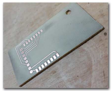
A printed circuit board such as the example in the image has only one conductive layer. A single-layer PCB is very restrictive; the circuit realization will not make efficient use of the available areas, and the designer may have difficulty creating the necessary interconnections.
*The Composition of A PCB Board
The base or substrate material of the printed circuit board where all the components and equipment on the printed circuit board are supported is usually fiberglass. If taken into account the data of PCB manufacturing, the most popular material for fiberglass is FR4. FR4 solid core provides the Printed Circuit Board its strength, support, rigidity, and thickness. Since there are different types of printed circuit boards like normal PCBs, flexible PCBs, etc. they are built using flexible high-temperature plastic.
Also read: PCB Design | PCB Manufacturing Process Flow Chart, PPT, and PDF
Why is it Called a Printed Circuit Board?
First Ever PCB Board
The invention of the printed circuit board is credited to Paul Eisler, an Austrian inventor. Paul Eisler first developed the printed circuit board when he was working on a radio set in 1936, but circuit boards did not see mass usage until after the 1950s. From then onwards, the popularity of PCBs began rapidly growing.
Printed circuit boards evolved from electrical connection systems that were developed in the 1850s, although the development leading up to the invention of the circuit board can be traced all the way back to the 1890s. Metal strips or rods were originally used to connect large electric components mounted on wooden bases.
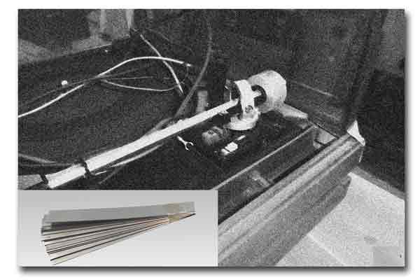
*Metal strips used in components connection
In time the metal strips were replaced by wires connected to screw terminals, and wooden bases were replaced by metal chassis. But smaller and more compact designs were needed due to the increased operating needs of the products that used circuit boards.
In 1925, Charles Ducas of the United States submitted a patent application for a method of creating an electrical path directly on an insulated surface by printing through a stencil with electrically conductive inks. This method gave birth to the name "printed wiring" or "printed circuit."
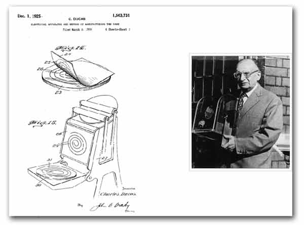
* Printed circuit board patents and Charles Ducas with the first radio set using a printed circuit chassis and aerial coil.
But the invention of the printed circuit board is credited to Paul Eisler, an Austrian inventor. Paul Eisler first developed the printed circuit board when he was working on a radio set in 1936, but circuit boards did not see mass usage until after the 1950s. From then onwards, the popularity of PCBs began rapidly growing.
The Development History of PCBs
● 1925: Charles Ducas, an American inventor, patents the first circuit board design when he stencils conductive materials onto a flat wooden board.
● 1936: Paul Eisler develops the first printed circuit board for use in a radio set.
● 1943: Eisler patents a more advanced PCB design that involves etching the circuits onto copper foil on glass-reinforced, non-conductive substrate.
● 1944: The United States and Britain work together to develop proximity fuses for use in mines, bombs, and artillery shells during WWII.
● 1948: The United States Army releases PCB technology to the public, prompting widespread development.
● 1950s: Transistors are introduced to the electronics market, reducing the overall size of electronics, and making it easier to incorporate PCBs and dramatically improving electronics reliability.
● 1950s-1960s: PCBs evolve into double-sided boards with electrical components on one side and identification printing on the other. Zinc plates are incorporated into PCB designs and corrosion-resistant materials and coatings are implemented to prevent degradation.
● 1960s: The integrated circuit – IC or silicon chip – is introduced into electronic designs, putting thousands and even tens of thousands of components on a single chip – significantly improving the power, speed, and reliability of electronics that incorporate these devices. To accommodate the new IC’s the number of conductors in a PCB had to increase dramatically, resulting in more layers within the average PCB. And at the same time, because the IC chips are so small, the PCBs begin to grow smaller, and soldering connections reliably becomes more difficult.
● 1970s: Printed circuit boards are incorrectly associated with the environmentally harmful chemical polychlorinated biphenyl, which was also abbreviated as PCB at the time. This confusion results in public confusion and community health concerns. To reduce confusion, printed circuit boards (PCBs) are renamed printed wiring boards (PWB) until chemical PCBs are phased out in the 1990s.
● 1970s – 1980s: Soldermasks of thin polymer materials are developed to facilitate easier solder application onto the copper circuits without bridging adjacent circuits, further increasing circuit density. A photo imageable polymer coating is later developed that can be applied directly to the circuits, dried, and modified by photo exposure afterward, further improving circuit density. This becomes a standard manufacturing method for PCBs.
● 1980’s: A new assembly technology is developed called surface mount technology – or SMT for short. Previously all PCB components had wire leads that were soldered into holes in the PCBs. These holes took up valuable real estate that was needed for additional circuit routing. SMT components were developed, and quickly became the manufacturing standard, that were soldered directly onto small pads on the PCB, without needing holes. SMT components proliferated quickly becoming the industry standard, and worked to replace through hole components, again improving functional power, performance, reliability as well as reducing electronic manufacturing costs.
● 1990s: PCBs continue to decrease in size as computer-aided design and manufacturing (CAD/CAM) software becomes more prominent. Computerization design automates many steps in PCB design, and facilitates increasingly complex designs with smaller, lighter components. The component suppliers work simultaneously to improve the performance of their devices, reduce their electrical consumption, increase their reliability, while at the same time reducing cost. Smaller connections allow for rapidly increasing PCB miniaturization.
● 2000s: PCBs have become smaller, lighter, much higher layer counts and more complex. Multi-layered and flexible circuit PCB designs allow for vastly more operational functionality in electronic devices, with increasingly smaller and lower cost PCBs.
Also read: How to Recycle A Waste Printed Circuit Board? | Things You Should Know
Different Types of PCBs (Printed Circuit Boards)
PCBs are often classified on the basis of frequency, the number of layers, and substrate used. Some poplar types are discussed below:
● Single-Sided PCBs / Single-layer PCBs
● Double-Sided PCBs / Double-layer PCBs
● Multi-layer PCBs
● Flexible PCBs
● Rigid PCBs
● Rigid-Flex PCBs
● High-Frequency PCBs
● Aluminum backed PCBs
1. Single-Sided PCBs / Single-layer PCBs
Single-sided PCBs are the basic type of circuit boards, which contain only one layer of substrate or base material. One side of the base material is coated with a thin layer of metal. Copper is the most common coating due to how well it functions as an electrical conductor. These PCBs also contain a protective solder mask, which is applied on the top of the copper layer along with a silkscreen coat.

*Single-layer PCB Diagram
Some advantages offered by single-sided PCB’s are:
● Single-sided PCBs are utilized for volume production and are low in cost.
● These PCBs are utilized for simple circuits such as power sensors, relays, sensors, and electronic toys.
The low-cost, high-volume model means they are commonly used for a variety of applications, including calculators, cameras, radio, stereo equipment, solid-state drives, printers, and power supplies.
<<Back to "Different Types of PCBs"
2. Double-Sided PCBs / Double-layer PCBs
Double-sided PCBs have both sides of the substrate featuring a metal conductive layer. Holes in the circuit board allow the metal parts to be attached from one side to the other. These PCBs connect the circuits on either side by either of the two mounting schemes, namely through-hole technology and surface mount technology. The through-hole technology involves inserting lead components through the pre-drilled holes on the circuit board, which are soldered to the pads on the opposite sides. The surface mount technology involves electrical components to be directly placed on the surface of the circuit boards.
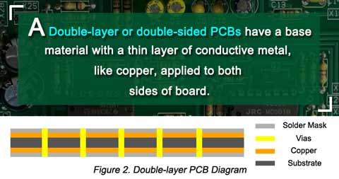
*Double-layer PCB Diagram
Advantages offered by double-sided PCBs are:
● Surface mounting allows more circuits to be attached to the board in comparison to the through-hole mounting.
● These PCBs are utilized in a wide range of applications, including mobile phone systems, power monitoring, test equipment, amplifiers, and many others.
Surface mount PCBs don't utilize wires as connectors. Instead, many small leads are soldered directly to the board, meaning that the board itself is used as a wiring surface for the different components. This allows circuits to be completed using less space, freeing up space to allow the board to complete more functions, usually at higher speeds and lighter weight than a through-hole board would allow.
Double-sided PCBs are typically used in applications that require an intermediate level of circuit complexity, such as industrial controls, power supplies, instrumentation, HVAC systems, LED lighting, automotive dashboards, amplifiers, and vending machines.
<<Back to "Different Types of PCBs"
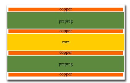
3. Multi-layer PCBs
Multi-layer PCBs have printed circuit boards, which comprise more than two copper layers like 4L, 6L, 8L, etc. These PCBs expand the technology used in double-sided PCBs. Various layers of a substrate board and insulating materials separate the layers in multi-layer PCBs. The PCBs are compact sized and offer benefits of weight and space.
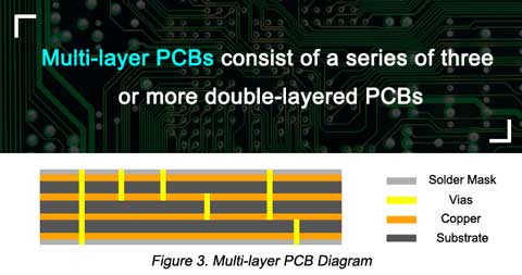
*Multi-layer PCB Diagram
Some advantages offered by multi-layer PCBs are:
● Multi-layer PCBs offer a high level of design flexibility.
● These PCBs play an important role in high-speed circuits. They provide more space for conductor patterns and power.
<<Back to "Different Types of PCBs"
4. Flexible PCBs
Flexible PCBs are constructed on a flexible base material. These PCBs come in single-sided, double-sided, and multilayer formats. This helps in reducing the complexity within the device assembly. Unlike rigid PCBs, which use unmoving materials such as fiberglass, flexible printed circuit boards are made of materials that can flex and move, such as plastic. Like rigid PCBs, flexible PCBs come in single, double, or multilayer formats. As they need to be printed on a flexible material, flexible PCB cost more for fabrication.
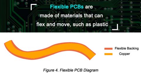
*Flexible PCB Diagram
Still, flexible PCBs offer many advantages over rigid PCBs. The most prominent of these advantages is the fact that they are flexible. This means they can be folded over edges and wrapped around corners. Their flexibility can lead to cost and weight savings since a single flexible PCB can be used to cover areas that might take multiple rigid PCBs.
Flexible PCBs can also be used in areas that might be subject to environmental hazards. To do so, they are simply built using materials that might be waterproof, shockproof, corrosion-resistant, or resistant to high-temperature oils - an option that traditional rigid PCBs may not have.
Some advantages offered by these PCBs are:
● Flexible PCBs help in decreasing the board size, which makes them ideal for various applications where high signal trace density is needed.
● These PCBs are designed for working conditions, where temperature and density are the main concern.
Flexible PCBs can also be used in areas that might be subject to environmental hazards. To do so, they are simply built using materials that might be waterproof, shockproof, corrosion-resistant, or resistant to high-temperature oils - an option that traditional rigid PCBs may not have.
<<Back to "Different Types of PCBs"
5. Rigid PCBs
Rigid PCBs refer to those types of PCBs whose base material is fabricated from a solid material and which cannot be bent. Rigid PCBs are made out of a solid substrate material that prevents the board from twisting. Possibly the most common example of a rigid PCB is a computer motherboard. The motherboard is a multilayer PCB designed to allocate electricity from the power supply while simultaneously allowing communication between all of the many parts of the computer, such as CPU, GPU, and RAM.
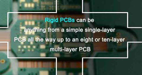
*Rigid PCBs can be anything from a simple single-layer PCB all the way up to an eight or ten-layer multi-layer PCB
Rigid PCBs make up perhaps the largest number of PCBs manufactured. These PCBs are used anywhere that there is a need for the PCB itself to be set up in one shape and remain that way for the remainder of the device's lifespan. Rigid PCBs can be anything from a simple single-layer PCB all the way up to an eight or ten-layer multi-layer PCB.
All Rigid PCBs have single-layer, double-layer, or multilayer constructions, so they all share the same applications.
● These PCBs are compact, which ensures the creation of a variety of complex circuitry around them.
● Rigid PCBs offer easy repair and maintenance, as all the components, are clearly marked. Also, the signal paths are well organized.
<<Back to "Different Types of PCBs"
Rigid-flex PCBs are a combination of rigid and flexible circuit boards. They comprise multiple layers of flexible circuits attached to more than one rigid board.
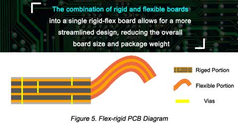
*Flex-rigid PCB Diagram
Some advantages offered by these PCBs are:
● These PCBs are precision-built. Hence, it is used in various medical and military applications.
● Being light-weight, these PCBs offer 60% of weight and space savings.
Flex-rigid PCBs are most often found in applications where space or weight are prime concerns, including Cell phones, Digital cameras, Pacemakers, and Automobiles.
<<Back to "Different Types of PCBs"
7. High-Frequency PCBs
High-frequency PCBs are used in the frequency range of 500MHz – 2GHz. These PCBs are used in various frequency critical applications like communication systems, microwave PCBs, microstrip PCBs, etc.
High-frequency PCB materials often include FR4-grade glass-reinforced epoxy laminate, polyphenylene oxide (PPO) resin, and Teflon. Teflon is one of the most expensive options available because of its small and stable dielectric constant, small amounts of dielectric loss, and overall low water absorption.
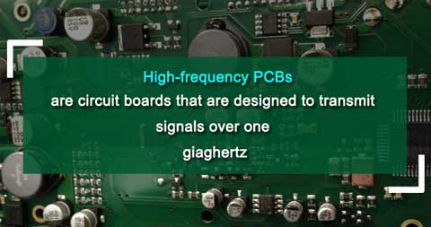
*High-frequency PCBs are citcuit boards that are designed to transmit signals over one giaghertz
Many aspects need to be considered when choosing a high-frequency PCB board and its corresponding type of PCB connector, including dielectric constant (DK), dissipation, loss, and dielectric thickness.
The most important of those is the Dk of the material in question. Materials with a high probability for the change of dielectric constant often have changes in impedance, which can disrupt the harmonics that make up a digital signal and cause an overall loss of digital signal integrity — one of the things that high-frequency PCBs are designed to prevent.
Other things to consider when choosing the boards and PC connector types to use when designing a high-frequency PCB are:
● Dielectric loss (DF), which affects the quality of signal transmission. A smaller amount of dielectric loss could make a small amount of signal wastage.
● Thermal expansion. If the thermal expansion rates of the materials used to build the PCB, such as copper foil, are not the same, then materials could separate from each other due to changes in temperature.
● Water absorption. High amounts of water intake will affect the dielectric constant and dielectric loss of PCB, especially if it is used in wet environments.
● Other resistances. The materials utilized in the construction of a high-frequency PCB should be rated highly for heat resistance, impact endurance, and resistance to hazardous chemicals, as necessary.
FMUSER is the expert in manufacturing High-frequency PCBs, we provide not only budget PCBs, but also online support for your PCBs design, contact us for more information!

<<Back to "Different Types of PCBs"
8. Aluminum backed PCBs
These PCBs are used in high-power applications, as the aluminum construction helps in heat dissipation. Aluminum-backed PCBs are known to offer a high level of rigidity and a low level of thermal expansion, which makes them ideal for applications having high mechanical tolerance.
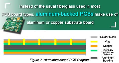
*Aluminum PCB Diagram
Some advantages offered by these PCBs are:
▲ Low cost. Aluminum is one of the most abundant metals on Earth, making up 8.23% of the planet's weight. Aluminum is easy and inexpensive to mine, which helps to cut expenses in the manufacturing process. Thus, building products with aluminum is less expensive.
▲ Environmentally friendly. Aluminum is non-toxic and easily recyclable. Due to its ease of assembly, manufacturing printed circuit boards out of aluminum is also a good way to conserve energy.
▲ Heat dissipation. Aluminum is one of the best materials available for dissipating heat away from crucial components of circuit boards. Instead of dispersing the heat out into the rest of the board, it transfers heat out into the open air. Aluminum PCB cools faster than an equivalent-sized copper PCB.
▲ Material durability. Aluminum is far more durable than materials like fiberglass or ceramic, especially for drop tests. The use of sturdier base materials helps reduce damage during manufacture, shipping, and installation.
All of these advantages make Aluminum PCB an excellent choice for applications that require high outputs of power within very tight tolerances, including traffic lights, automotive lighting, power supplies, motor controllers, and high-current circuitry.
In addition to LEDs and power supplies. aluminum-backed PCBs can also be used in applications that require a high degree of mechanical stability or where the PCB might be subject to high levels of mechanical stress. They are less subject to thermal expansion than a fiberglass-based board, meaning that the other materials on the board, such as the copper foil and insulation, will be less likely to peel away, further lengthening the lifetime of the product.
<<Back to "Different Types of PCBs"
▲BACK▲
Printed Circuit Board Industry in 2021
The global PCB market can be segmented on the basis of product type into flex (flexible FPCB and rigid-flex PCB), IC substrate, high density interconnect (HDI), and others. On the basis of PCB laminate type, the market can be split into PR4, High Tg Epoxy, and Polyimide. The market can be divided on the basis of applications into consumer electronics, automotive, medical, industrial, and military/ aerospace, etc.
The growth of the PCB market over the historic period has been supported by various factors such as the booming consumer electronics market, growth in the healthcare devices industry, increased need for double-sided PCB, a spike in demand for hi-tech features in automotive, and a hike in disposable income. The market is also faced with some challenges such as strict supply chain controls and inclination towards COTS components.
The Printed Circuit Board market is expected to register a CAGR of 1.53% during the forecast period (2021 - 2026) and was valued at USD 58.91 billion in 2020, and it is projected to be worth USD 75.72 billion by 2026 during the period 2021-2026. The market experienced rapid growth in the last few years, primarily owing to the continuous development of consumer electronics devices and increasing demand for PCBs in all electronics and electrical equipment.
The adoption of PCBs in connected vehicles has also accelerated the PCB market. These are vehicles that are fully equipped with both wired and wireless technologies, which make it possible for the vehicles to connect to computing devices like smartphones at ease. With such technology, drivers are able to unlock their vehicles, start climate control systems remotely, check their electric cars' battery status, and track their cars using smartphones.
The proliferation of 5G technology, 3D printed PCB, other innovations such as biodegradable PCB, and the spike in the use of PCB in wearable technologies and mergers and acquisitions (M&A) activity are some of the latest trends existing in the market.
Additionally, the demand for electronic devices, such as smartphones, smartwatches, and other devices, has also boosted the market’s growth. For instance, According to the US Consumer Technology Sales and Forecast study, which was conducted by the Consumer Technology Association (CTA), the revenue generated by smartphones was valued at USD 79.1 billion and USD 77.5 billion in 2018 and 2019, respectively.
3D printing has proved integral to one of the big PCB innovations lately. 3D-printed electronics, or 3D PEs, are expected to revolutionize the way electrical systems are designed in the future. These systems create 3D circuits by printing a substrate item layer by layer, then adding a liquid ink on top of it that contains electronic functionalities. Surface-mount technologies can then be added to create the final system. 3D PE can potentially provide immense technical and manufacturing benefits for both circuit manufacturing companies and their clients, especially compared to traditional 2D PCBs.
With the outbreak of COVID-19, the production of printed circuit boards was impacted by constraints and delays in the Asia-Pacific region, especially in China, during the months of January and February. Companies have not made major changes to their production capacities but weak demand in China presents some supply chain issues. The Semiconductor Industry Association (SIA) report, in February, indicated potential longer-term business impacts outside of China related to the COVID-19. The effect of diminished demand could be reflected in companies' 2Q20 revenues.
The growth of the PCB market is strongly linked to the global economy and structural technology like smartphones, 4G/5G, and data centers. The downfall in the market in 2020 is expected due to the impact of Covid-19. The pandemic has put the brakes on the manufacturing of consumer electronics, smartphones, and automotive and thus dampened demand for PCBs. The market would showcase gradual recovery owing to the resumption of manufacturing activities to give a trigger pulse to the global economy.
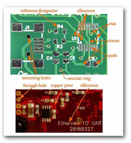
What is A Printed Circuit Board Made of?
PCB is generally made from four layers of material bonded together by heat, pressure, and other methods. Four layers of a PCB are made of substrate, copper, solder mask, and silkscreen.
Each board will be different, but they will mostly share some of the elements, here are a few of the most common materials used in the fabrication of printed circuit boards:
The six basic components of a standard printed circuit board are:
● The core layer – contains glass fiber reinforced epoxy resin
● A conductive layer – contains traces and pads to make up the circuit (usually with copper, gold, silver)
● Solder mask layer – thin polymer ink
● Silkscreen overlay – special ink that shows the component references
● A tin solder – used to attach components to through-holes or surface mount pads
Prepreg
Prepreg is a thin glass fabric that is coated with resin and dried, in special machines called prepreg treaters. The glass is the mechanical substrate that holds the resin in place. The resin – usually FR4 epoxy, polyimide, Teflon, and others – starts as a liquid that is coated onto the fabric. As the prepreg moves through the treater, it enters an oven section and begins to dry. Once it exits the treater, it is dry to the touch.
When prepreg is exposed to higher temperatures, usually above 300º Fahrenheit, the resin begins to soften and melt. Once the resin in the prepreg melts, it reaches a point (called thermosetting) where it then re-hardens to become rigid again and very, very strong. Despite that strength, prepreg and laminate tend to be very light. Prepreg sheets, or fiberglass, are used to manufacture many things – from boats to golf clubs, aircraft, and wind turbine blades. But it is also critical in PCB manufacturing. Prepreg sheets are what we use to glue the PCB together, and they are also what is used to build the second component of a PCB – laminate.
*PCB stack up-side-view diagram
Laminate
Laminates, sometimes called copper-clad laminates, are created by curing under high temperatures and pressure layers of cloth with a thermoset resin. This process forms the uniform thickness that is essential to the PCB. Once the resin hardens, PCB laminates are like a plastic composite, with sheets of copper foil on both sides, if your board has a high layer count, then the laminate must be made up of woven glass for dimensional stability.
RoHS Compliant PCB
RoHS Compliant PCBs are those that follow the Restriction of Hazardous Substances from the European Union. The ban is on the use of lead and other heavy metals in consumer products. Every part of the board must be free of lead, mercury, cadmium, and other heavy metals.
Soldermask
Soldermask is the green epoxy coating that covers the circuits on the outer layers of the board. The internal circuits are buried in the layers of prepreg, so they do not need to be protected. But the external layers, if left unprotected, will oxidize and corrode over time. Soldermask provides that protection to the conductors on the outside of the PCB.
Nomenclature - Silkscreen
Nomenclature, or sometimes called silkscreen, is the white letters that you see on top of the solder mask coating on a PCB. The silkscreen is usually the final layer of the board, which allows the PCB manufacturer to write labels on the important areas of the board. It is a special ink that shows the symbols and component references for the component locations during the assembly process. Nomenclature is the lettering that shows where each component goes on the board and sometimes provides component orientation as well.
Both solder masks and nomenclature are typically green and white, though you may see other colors like red, yellow, gray, and black used, those are the most popular.
Soldermask protects all the circuits on the outer layers of the PCB, where we do not intend to attach components. But we also need to protect the exposed copper holes and pads where we plan to solder and mount the components. To protect those areas, and to provide a good solderable finish, we usually use metallic coatings, such as nickel, gold, tin/lead solder, silver, and other final finishes designed just for PCB manufacturers.
▲BACK▲
Most Popular PCBs Designed Fabricated Material
PCB designers face several performance features when they look at material selection for their design. Some of the most popular considerations are:
Dielectric constant – a key electrical performance indicator
Flame retardance – critical for UL qualification (see above)
Higher glass transition temperatures (Tg) – to withstand higher temperature assembly processing
Mitigated loss factors – important in high-speed applications, where signal speed is valued
Mechanical strength including shear, tensile and other mechanical attributes that may be required of the PCB when placed into service
Thermal performance – an important consideration in elevated service environments
Dimensional stability – or how much does the material move, and how consistently does it move, during manufacturing, thermal cycles, or exposure to humidity
Here are a few of the most popular materials used in the fabrication of printed circuit boards:
The substrate: FR4 epoxy laminate and prepreg - fiberglass
FR4 is the most popular PCB substrate material in the world. The denotation ‘FR4’ describes a class of materials that meet certain requirements defined by NEMA LI 1-1998 standards. FR4 materials have good thermal, electrical, and mechanical characteristics, as well as a favorable strength-to-weight ratio that makes them ideal for most electronic applications. FR4 laminates and prepreg are made from glass cloth, epoxy resin, and are usually the lowest cost PCB material available. It can also be made from flexible materials which sometimes can be stretched, too.
It is especially popular for PCBs with lower layer counts – single, double-sided into multilayered constructions generally less than 14 layers. Additionally, the base epoxy resin can be blended with additives that can significantly improve its thermal performance, electrical performance, and UL flame survival/rating – greatly improving its ability to be used in higher-layer count builds higher thermal stress applications and greater electrical performance at a lower cost for high-speed circuit designs. FR4 laminates and prepregs are very versatile, adaptable with widely accepted manufacturing techniques with predictable yields.
Polyimide laminates and prepreg
Polyimide laminates offer higher temperature performance than FR4 materials as well as a slight improvement in electrical performance properties. Polyimides materials cost more than FR4 but offer improved survivability in harsh and higher temperature environments. They also are more stable during thermal cycling, with fewer expansion characteristics, making them suitable for higher-layer count constructions.
Teflon(PTFE) laminates and bonding plies
Teflon laminates and bonding materials offer excellent electrical properties, making them ideal for high-speed circuitry applications. Teflon materials are more expensive than polyimide but provide designers with the high-speed capabilities that they need. Teflon materials can be coated onto glass fabric, but can also be manufactured as an unsupported film, or with special fillers and additives to improve mechanical properties. Manufacturing Teflon PCBs often requires a uniquely skilled workforce, specialized equipment and processing, and an anticipation of lower manufacturing yields.
Flexible laminates
Flexible laminates are thin and provide the ability to fold the electronic design, without losing electrical continuity. They do not have glass fabric for support but are built on plastic film. They are equally effective folded into a device for a one-time flex to install application, as they are in dynamic flex, where the circuits will be folded continuously for the life of the device. Flexible laminates can be made from higher temperature materials like polyimide and LCP (liquid crystal polymer), or very low-cost materials such as polyester and PEN. Because the flexible laminates are so thin, manufacturing flexible circuits also can require a uniquely skilled workforce, specialized equipment and processing, and an anticipation of lower manufacturing yields.
Others
There are many other laminates and bonding materials on the marketplace including BT, cyanate ester, ceramics, and blended systems that combine resins to get distinct electrical and/or mechanical performance characteristics. Because the volumes are so much lower than FR4, and the manufacturing can be much more difficult, they are usually considered expensive alternatives for PCB designs.
The printed circuit board assembly process is a complex one involving interaction with many small components and detailed knowledge of each part’s functions and placement. A circuit board will not function without its electrical components. In addition, different components are used depending on the device or product it is intended for. As such, it is important to have an in-depth understanding of the different components that go into printed circuit board assembly.
▲BACK▲
Printed Circuit Board Components and How they Work
The following 13 common components are used in most printed circuit boards:
● Resistors
● Transistors
● Capacitors
● Inductors
● Diodes
● Transformers
● Integrated Circuits
● Crystal Oscillators
● Potentiometers
● SCR(Silicon-Controlled Rectifier)
● Sensors
● Switches/Relays
● Batteries
1. Resistors - Energy Controlling
Resistors are one of the most commonly used components in PCBs and are probably the simplest to understand. Their function is to resist the flow of current by dissipating electric power as heat. Without resistors, other components may not be able to handle the voltage and this may result in overloading. They come in a multitude of different types made of a range of different materials. Classic resistor most familiar to the hobbyist is the ‘axial’ style resistors with leads on both long ends and the body inscribed with colored rings.
2. Transistors - Energy Amplifying
Transistors are crucial to the printed circuit board assembly process due to their multi-functional nature. They are semiconductor devices that can both conduct and insulate and can act as switches and amplifiers. They are smaller in size, have a relatively long life, and can operate at lower voltage supplies safely without a filament current. Transistors come in two types: bipolar junction transistors (BJT) and field-effect transistors (FET).
3. Capacitors - Energy Storing
Capacitors are passive two-terminal electronic components. They act like rechargeable batteries – to temporarily hold electric charge, and release it whenever more power is needed elsewhere in the circuit.
You can do this by collecting opposite charges on two conductive layers separated by an insulating, or dielectric, material.
Capacitors are often categorized according to the conductor or dielectric material, which gives rise to many types with varying characteristics from high capacitance electrolytic capacitors, diverse polymer capacitors to the more stable ceramic disc capacitors. Some have appearances similar to axial resistors, but the classic capacitor is a radial style with the two leads protruding from the same end.
4. Inductors - Energy Increasing
Inductors are passive two-terminal electronic components that store energy(instead of storing electrostatic energy) in a magnetic field when an electric current passes through them. Inductors are used to block alternating currents while allowing direct currents to pass.
Inductors are often used to filter out or block certain signals, for example, blocking interference in radio equipment or used in conjunction with capacitors to make tuned circuits, to manipulate AC signals in switched-mode power supplies, ie. TV receiver.
5. Diodes - Energy Redirecting
Diodes are semiconductor components that act as one-way switches for currents. They allow currents to pass easily in one direction that allows current to flow in one direction only, from the anode (+) to the cathode (-) but restrict currents from flowing in the opposite direction, which could cause damage.
The most popular diode with hobbyists is the light-emitting diode or LED. As the first part of the name suggests, they are used to emit light, but anyone who has tried to solder one knows, it is a diode, so it is important to get the orientation correct, otherwise, the LED won’t light up.
6. Transformers - Energy Transfering
The function of transformers is to transfer electrical energy from one circuit to another, with an increase or decrease in voltage. General transformers transfer power from one source to another through a process called “induction.” As with resistors, they technically regulate current. The biggest difference is that they provide more electrical isolation than controlled resistance by “transforming” the voltage. You may have seen large industrial transformers on telegraph poles; these step-down the voltage from overhead transmission lines, typically several hundred thousand volts, to the few hundred volts typically required for household use.
PCB transformers consist of two or more separate inductive circuits (called windings) and a soft iron core. The primary winding is for the source circuit—or where the energy will come from—and the secondary winding is for the receiving circuit—where the energy is going. Transformers break down large amounts of voltage into smaller, more manageable currents so as not to overload or overwork the equipment.
7. Integrated Circuits - Powerhouses
ICs or integrated circuits are circuits and components that have been shrunk down onto wafers of semiconductor material. The sheer number of components that can be fit onto a single chip is what gave rise to the first calculators and now powerful computers from smartphones to supercomputers. They are usually the brains of a wider circuit. The circuit is typically encased in a black plastic housing which can come in all shapes and sizes and have visible contacts, whether they are leads extending out from the body, or contact pads directly under like BGA chips for example.
8. Crystal Oscillators - Precise Timers
Crystal oscillators provide the clock in many circuits that require precise and stable timing elements. They produce a periodic electronic signal by physically causing a piezoelectric material, the crystal, to oscillate, hence the name. Each crystal oscillator is designed to vibrate at a specific frequency and is more stable, economical, and has a small form factor compared to other timing methods. For this reason, they are commonly used as precise timers for microcontrollers or more commonly, in quartz wristwatches.
9. Potentiometers - Varied Resistance
Potentiometers are a form of variable resistor. They are commonly available in rotary and linear types. By rotating the knob of a rotary potentiometer, resistance is varied as the slider contact is moved over a semi-circular resistor. A classic example of rotary potentiometers is the volume controller on radios where the rotary potentiometer controls the amount of current to the amplifier. The linear potentiometer is the same, except that resistance is varied by moving the slider contact on the resistor linearly. They are great when fine-tuning is required in the field.
10. SCR(Silicon-Controlled Rectifier) - High Current Control
Also known as thyristors, Silicon Controlled Rectifiers (SCR) are similar to transistors and diodes – in fact, they are essentially two transistors working together. They also have three leads but consist of four silicon layers instead of three and only function as switches, not amplifiers. Another important difference is that only a single pulse is required to activate the switch, whereas the current has to be applied continuously in the case of a single transistor. They are more suited to switching larger amounts of power.
11. Sensors
Sensors are devices whose function is to detect changes in environmental conditions and generate an electrical signal corresponding to that change, which is sent to other electronic components in the circuit. Sensors convert energy from a physical phenomenon into electrical energy, and so they are in effect, transducers (convert energy in one form into another). They can be anything from a type of resistor in a resistance temperature detector (RTD), to LEDs detecting in-fared signals, such as in a television remote. A wide variety of sensors exist for various environmental stimuli for example humidity, light, air quality, touch, sound, moisture, and motion sensors.
12. Switches and Relays - Power Buttons
A basic and easily overlooked component, the switch is simply a power button to control the current flow in the circuit, by switching between an open or a closed circuit. They vary quite a bit in physical appearance, ranging from the slider, rotary, push button, lever, toggle, key switches and the list goes on. Similarly, a relay is an electromagnetic switch operated via a solenoid, which becomes like a sort of temporary magnet when current flows through it. They function as switches and can also amplify small currents to larger currents.
13. Batteries - Energy Providing
In theory, everyone knows what a battery is. Perhaps the most widely-purchased component on this list, batteries are used by more than just electronic engineers and hobbyists. People use this little device to power their everyday objects; remotes, flashlights, toys, chargers, and more.
On a PCB, a battery basically stores chemical energy and converts it into usable electronic energy to power the different circuits present on the board. They use an external circuit to allow electrons to flow from one electrode to the other. This forms a functional (but limited) electric current.
The current is limited by the conversion process of chemical energy to electrical energy. For some batteries, this process could finish in a matter of days. Others might take months or years before the chemical energy is completely spent. This is why some batteries (like the batteries in remotes or controllers) need to be changed every few months whereas others (like wrist watch batteries) take years before they’re all used up.
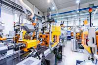
PCBs are found in nearly every electronic and computing device, including motherboards, network cards, and graphics cards to internal circuitry found in hard/CD-ROM drives. In terms of computing applications where fine conductive traces are needed such as laptops and desktops, they serve as the foundation for many internal computer components, such as video cards, controller cards, network interface cards, and expansion cards. These components all connect to the motherboard, which is also a printed circuit board.
PCBs are also made by a photolithographic process in a larger-scale version of the way conductive paths in processors are made.
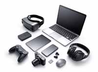
While PCBs are often associated with computers, they are used in many other electronic devices besides PCs. For example, most TVs, radios, digital cameras, cellphones, and tablets include one or more printed circuit boards. However, PCBs found in mobile devices look similar to those found in desktop computers and large electronics, but they are typically thinner and contain finer circuitry.
Still, the printed circuit board is widely used in almost all the precise equipment/devices, from small consumer devices to huge pieces of machinery, FMUSER hereby provides a list of top 10 common uses of PCB (printed circuit board) in daily lives.
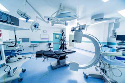
● Medical imaging systems
● Monitors
● Infusion pumps
● Internal devices
● Medical imaging systems: CT, CAT and ultrasonic scanners often use PCBs, as do the computers that compile and analyze these images.
● Infusion pumps: Infusion pumps, such as insulin and patient-controlled analgesia pumps, deliver precise amounts of a fluid to a patient. PCBs help ensure these products function reliably and accurately.
● Monitors: Heart rate, blood pressure, blood glucose monitors and more depend on electronic components to obtain accurate readings.
● Internal devices: Pacemakers and other devices that are used internally require small PCBs to function.
Conclusion:
The medical sector is continually coming up with more uses for electronics. As technology improves and smaller, denser, more reliable boards become possible, PCBs will play an increasingly important role in healthcare.
● Communications equipment:
● Control systems:
● Instrumentation:
● Communications equipment: Radio communication systems and other critical communications require PCBs to function.
● Control systems: PCBs are at the center of the control systems for various types of equipment including radar jamming systems, missile detection systems and more.
● Instrumentation: PCBs enable indicators that members of the military use to monitor threats, conduct military operations and operate equipment.
Conclusion:
The military is often at the cutting edge of technology, so some of the most advanced uses of PCBs are for military and defense applications. The uses of PCBs in the military vary widely.
Application
Example
Medical Devices
Application
Example
Military and Defense Applications

● Security cameras:
● Smoke detectors:
● Electronic door locks
● Motion sensors and burglar alarms
● Smoke detectors: Smoke detectors as well as other similar devices, such as carbon monoxide detectors, need reliable PCBs to function.
● Electronic door locks: Modern electronic door locks also incorporate PCBs.
● Motion sensors and burglar alarms: Security sensors that detect motion rely on PCBs as well.
Conclusion:
PCBs play an essential role in many different types of security equipment, especially as more of these types of products are gaining the ability to connect to the Internet.
Application
Example
Safety and Security Equipment
 ● Security cameras: Security cameras, whether used indoors or outdoors, rely on PCBs, as does equipment used to monitor security footage.
● Residential lighting
● Automotive displays
● Computer displays
● Medical lighting
● Storefront lighting
● Storefront lighting: Businesses can use LEDs for signage and to light their stores.
● Automotive displays: Dashboard indicators, headlights, brake lights and more may use LED PCBs.
● Computer displays: LED PCBs power many indicators and displays on laptop and desktop computers.
● Medical lighting: LEDs provide bright light and give off little heat, making them ideal for medical applications, especially those related to surgery and emergency medicine.
Conclusion:
LEDs are becoming increasingly common in a variety of applications, meaning PCBs will likely continue to play a more prominent role in lighting.
Application
Example
LEDs
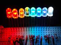 ● Residential lighting: LED lighting, including smart bulbs, help homeowners light their property more efficiently.
● Power supplies
● Monitoring equipment:
● Communication equipment
● Power supplies: PCBs are a key component in the equipment that powers a variety of aircraft, control tower, satellite and other systems.
● Monitoring equipment: Pilots use various kinds of monitoring equipment, including accelerometers and pressure sensors, to monitor the function of the aircraft. These monitors often use PCBs.
● Communication equipment: Communication with ground control is a vital part of ensuring safe air travel. These critical systems rely on PCBs.
Conclusion:
The electronics used in aerospace applications have similar requirements to those used in the automotive sector, but aerospace PCBs may be exposed to even harsher conditions. PCBs may be used in a variety of aerospace equipment including planes, space shuttles, satellites and radio communications systems.
Application
Example
Aerospace Components

| Application | Example |
|
Industrial Equipment |
● Manufacturing equipment
● Power equipment
● Measuring equipment
● Internal devices |
|
● Manufacturing equipment: PCB-based electronics power electric drills and presses used in manufacturing.
● Power equipment: The components that power many types of industrial equipment use PCBs. This power equipment includes DC-to-AC power inverters, solar power cogeneration equipment and more.
● Measuring equipment: PCBs often power equipment that measures and controls pressure, temperature and other factors.
Conclusion: As robotics, industrial IoT tech and other types of advanced technology become more common, new uses for PCBs are arising in the industrial sector. |
|
● Navigation systems
● Communications systems
● Control systems
● Navigation systems: Many maritime vessels rely on PCBs for their navigation systems. You can find PCBs in GPS and radar systems as well as other equipment.
● Communications systems: The radio systems that crews use to communicate with ports and other ships require PCBs.
● Control systems: Many of the control systems in maritime vessels, including engine management systems, power distribution systems and autopilot systems, use PCBs.
Conclusion:
These autopilot systems may help with boat stabilization, maneuvering, minimizing heading error and managing rudder activity.
Applications
Example
Maritime Applications

| Application | Example |
|
Consumer Electronics |
● Communications devices
● Computers
● Entertainment systems
● Home appliances |
|
● Communications devices: Smartphones, tablets, smartwatches, radios and other communications products require PCBs to function. ● Computers: Computers for both personal and business feature PCBs. ● Entertainment systems: Entertainment-related products such as televisions, stereos and video game consoles all rely on PCBs. ● Home appliances: Many home appliances also have electronic components and PCBs including refrigerators, microwaves and coffee makers.
Conclusion: The use of PCBs in consumer products is certainly not slowing down. The proportion of Americans who own a smartphone is now 77 percent and growing. Many devices that weren’t electronic before are now also gaining advanced electronic functionality and becoming part of the Internet of Things (IoT). |
|
| Application | Example |
|
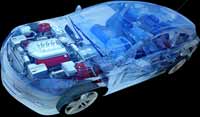
Automotive Components |
● Entertainment and navigation systems
● Control systems ● Sensors |
|
● Control systems: Many systems that control the basic functions of the car rely on electronics powered by PCBs. These include engine management systems and fuel regulators.
● Sensors: As cars become more advanced, manufacturers are incorporating more and more sensors. These sensors can monitor blind spots and warn drivers of nearby objects. PCBs are also necessary for the systems that enable cars to automatically parallel park.
Conclusion: These sensors are part of what enable cars to be self-driving. Fully autonomous vehicles are expected to become common in the future which is why a large number of printed circuit boards are used. |
|
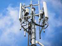
● Telecom towers
● Office communications equipment
● LED displays and indicators
● Telecom towers: Cell towers receive and transmit signals from cell phones and require PCBs that can withstand outdoor environments.
● Office communications equipment: Much of the communication equipment you might find in an office requires PCBs, including phone switching systems, modems, routers and Voice over Internet Protocol (VoIP) devices.
● LED displays and indicators: Telecom equipment often includes LED displays and indicators, which utilize PCBs.
Conclusion:
The telecom industry is constantly evolving, and so are the PCBs the sector uses. As we generate and transfer more data, powerful PCBs will become even more important for communications.
Application
Example
Telecommunications Equipment
FMUSER knows that any industry that uses electronic equipment requires PCBs. Whatever application you’re using your PCBs for, it’s important that they’re reliable, affordable, and designed to fit your needs.
As the expert in manufacturing PCBs of FM radio transmitter as well as the provider of audio and video transmission solutions, FMUSER also knows that you're looking for quality&budget PCBs for your FM broadcast transmitter, that's what we provide, contact us immediately for free PCB board inquiries!

▲BACK▲
PCB Assembly Principle: Through-Hole vs. Surface Mounted
In recent years, especially in the semiconductor field, increased demand for greater functionality, smaller size, and added utility is needed. And there are two methods of placing components on a printed circuit board (PCB), which is the Through-Hole Mounting (THM) and the Surface Mount Technology (SMT)., they vary in different features, advantages, and disadvantages, let's take a look!
Through-Hole Components
There are two types of through-hole mounting components:
Axial lead components - run through a component in a straight line (along the “axis”), with the end of the lead wire exiting the component on either end. Both ends are then placed through two separate holes on the board, providing the component with a closer, flatter fit. These components are preferred when looking for a snug, compact fit. Axial lead configuration may come in the form of carbon resistors, electrolytic capacitors, fuses, and light-emitting diodes (LEDs).
Radial lead components - protrude from the board, with its leads located on one side of the component. Radial leads occupy less surface area, making them preferable for high-density boards. Radial components are available as ceramic disk capacitors.
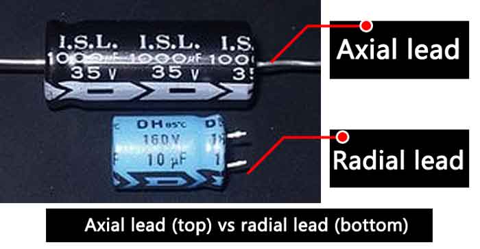
*Axial Lead (top) vs. Radial Lead (bottom)
Axial lead components run through a component in a straight line ("axially"), with each end of the lead wire exiting the component on either end. Both ends are then placed through two separate holes in the board, allowing the component to fit closer, flatter fit.
Generally, the axial lead configuration may come in the form of carbon resistors, electrolytic capacitors, fuses, and light-emitting diodes (LEDs).
Radial lead components, on the other hand, protruding from the board, as its leads are located on one side of the component. Both through-hole component types are "twin" lead components.
Radial lead components are available as ceramic disk capacitors while the axial lead configuration may come in the form of carbon resistors, electrolytic capacitors, fuses, and light-emitting diodes (LEDs).
And axial lead components are used for their snugness to the board, radial leads occupy less surface area, making them better for high-density boards
Through-Hole Mounting (THM)
Through-hole mounting is the process by which component leads are placed into drilled holes on a bare PCB, it is kind of the predecessor of Surface Mount Technology. The through-hole mounting method, in a modern assembly facility, but is still being considered a secondary operation and being used since the introduction of second-generation computers.
The process was standard practice until the rise of surface mount technology (SMT) in the 1980s, at which time it was expected to completely phase out through-hole. Yet, despite a severe drop in popularity over the years, through-hole technology has proven resilient in the age of SMT, offering a number of advantages and niche applications: namely, reliability, and that's why through-hole mounting replaces the old point-to-point construction.
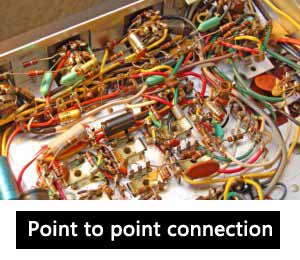
*Point to Point Connection
Overall, through-holes complete disappearance from PCB assembly is a wide misconception. Barring the above uses for through-hole technology, one should always keep in mind the factors of availability and cost. Not all components are available as SMD packages, and some through-hole components are less expensive.
Also read: Through Hole vs Surface Mount | What is the Difference?
Surface Mount Technology (SMT)
SMT the process by which components are mounted directly onto the surface of the PCB.
The surface Mount technology was known originally as “planar mounting,” around 1960 and became widely used in the mid-80s.
Nowadays, virtually all electronic hardware is manufactured using SMT. It has become essential to PCB design and manufacturing, having improved the quality and performance of PCBs overall, and has reduced the costs of processing and handling greatly.
The components used for surface mount technology are so-called Surface Mount Packages (SMD). These components have leads beneath or around the package.
There are many different types of SMD packages with different shapes and made of different materials. These types of packages are divided into different categories. The category “Rectangular Passive Components” includes mostly the standard SMD resistors and capacitors. The categories “Small Outline Transistor” (SOT) and “Small Outline Diode” (SOD), are used for transistors and diodes. There are also packages that are mostly used for Integrated Circuits (ICs) like Op-Amps, Transceivers, and Microcontrollers. Examples of packages that are used for ICs are: “Small outline Integrated Circuit” (SOIC), “Quad Flat Pack” (QFN), and “Ball Grid Array” (BGA).
The packages mentioned above are just some examples of the SMD packages that are available. There are many more types of packages with different variants available on the market.
The key differences between SMT and through-hole mounting are
(a) SMT does not require holes to be drilled through a PCB
(b) SMT components are much smaller
(c) SMT components can be mounted on both sides of the board.
The ability to fit a high number of small components on a PCB has allowed for much denser, higher performing, and smaller PCBs.
In a word: the biggest difference in comparison to through-hole mounting is that there is no need to drill holes in the PCB to create a connection between the tracks on the PCB and the components.
The leads of the component will make direct contact with the so-called PADs on a PCB.
Through-hole component leads, which run through the board and connect a board’s layers, have been replaced by "vias" -- small components which allow a conductive connection between the different layers of a PCB, and which essentially act as through-hole leads. Some surface mount components like BGAs are higher performing components with shorter leads and more interconnection pins that allow for higher speeds.
▲BACK▲
Sharing is Caring!