
Products Category
- FM Transmitter
- 0-50w 50w-1000w 2kw-10kw 10kw+
- TV Transmitter
- 0-50w 50-1kw 2kw-10kw
- FM Antenna
- TV Antenna
- Antenna Accessory
- Cable Connector Power Splitter Dummy Load
- RF Transistor
- Power Supply
- Audio Equipments
- DTV Front End Equipment
- Link System
- STL system Microwave Link system
- FM Radio
- Power Meter
- Other Products
- Special for Coronavirus
Products Tags
Fmuser Sites
- es.fmuser.net
- it.fmuser.net
- fr.fmuser.net
- de.fmuser.net
- af.fmuser.net ->Afrikaans
- sq.fmuser.net ->Albanian
- ar.fmuser.net ->Arabic
- hy.fmuser.net ->Armenian
- az.fmuser.net ->Azerbaijani
- eu.fmuser.net ->Basque
- be.fmuser.net ->Belarusian
- bg.fmuser.net ->Bulgarian
- ca.fmuser.net ->Catalan
- zh-CN.fmuser.net ->Chinese (Simplified)
- zh-TW.fmuser.net ->Chinese (Traditional)
- hr.fmuser.net ->Croatian
- cs.fmuser.net ->Czech
- da.fmuser.net ->Danish
- nl.fmuser.net ->Dutch
- et.fmuser.net ->Estonian
- tl.fmuser.net ->Filipino
- fi.fmuser.net ->Finnish
- fr.fmuser.net ->French
- gl.fmuser.net ->Galician
- ka.fmuser.net ->Georgian
- de.fmuser.net ->German
- el.fmuser.net ->Greek
- ht.fmuser.net ->Haitian Creole
- iw.fmuser.net ->Hebrew
- hi.fmuser.net ->Hindi
- hu.fmuser.net ->Hungarian
- is.fmuser.net ->Icelandic
- id.fmuser.net ->Indonesian
- ga.fmuser.net ->Irish
- it.fmuser.net ->Italian
- ja.fmuser.net ->Japanese
- ko.fmuser.net ->Korean
- lv.fmuser.net ->Latvian
- lt.fmuser.net ->Lithuanian
- mk.fmuser.net ->Macedonian
- ms.fmuser.net ->Malay
- mt.fmuser.net ->Maltese
- no.fmuser.net ->Norwegian
- fa.fmuser.net ->Persian
- pl.fmuser.net ->Polish
- pt.fmuser.net ->Portuguese
- ro.fmuser.net ->Romanian
- ru.fmuser.net ->Russian
- sr.fmuser.net ->Serbian
- sk.fmuser.net ->Slovak
- sl.fmuser.net ->Slovenian
- es.fmuser.net ->Spanish
- sw.fmuser.net ->Swahili
- sv.fmuser.net ->Swedish
- th.fmuser.net ->Thai
- tr.fmuser.net ->Turkish
- uk.fmuser.net ->Ukrainian
- ur.fmuser.net ->Urdu
- vi.fmuser.net ->Vietnamese
- cy.fmuser.net ->Welsh
- yi.fmuser.net ->Yiddish
What is Intrinsic Semiconductor and Extrinsic Semiconductor – Energy Band & Doping?
Date:2021/10/18 21:55:58 Hits:
Semiconductor, as the name suggests is a kind of material whose shows properties of both conductors and insulators. A semiconductor material requires a certain level of voltage or heat to release its carriers for conduction. These semiconductors are classified as ‘intrinsic’ and ‘extrinsic’ based on the number of carriers. The intrinsic carrier is the purest form of semiconductor and an equal number of electrons (negative charge carriers) and holes (positive charge carriers). The semiconductor materials most profoundly used are Silicon (Si), Germanium (Ge), and Gallium Arsenide (GaAs). Let us study the characteristics and behavior of these types of semiconductors.What is an Intrinsic Semiconductor?The Intrinsic semiconductor can be defined as chemically pure material without any doping or impurity added to it. The most commonly known intrinsic or pure semiconductors available are Silicon (Si) and Germanium (Ge). The behavior of the semiconductor on applying a certain voltage is dependent on its atomic structure. The outermost shell of both Silicon and Germanium have four electrons each. To stabilize each other nearby atoms form covalent bonds based on the sharing of valence electrons. This bonding in the crystal lattice structure of Silicon is illustrated in figure 1. Here it can be seen that the valence electrons of two Si atom pair together to form a Covalent Bond. 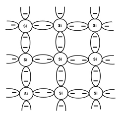 Figure 1. Covalent bonding of the Silicon atomAt all the covalent bonds are stable and no carriers are available for conduction. Here the intrinsic semiconductor behaves as an insulator or non-conductor. Now if the ambient temperature comes close to the room temperature of the covalent bonds start breaking. Thus the electrons from the valence shell are released to take part in conduction. As more number of carriers are released for conduction the semiconductor starts behaving as a conducting material. The energy band diagram given below explains this transition of carriers from the valence band to the conduction band.The Energy band diagramThe Energy band diagram shown in figure 2(a) depicts two levels, Conduction Band and Valence Band. The space between the two bands is called the forbidden gap
 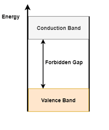 Figure 2 (a). Energy band diagram Figure
 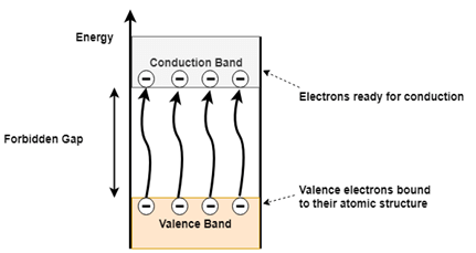 Figure 2(b). Conduction and Valence band electrons in a semiconductor When a semiconductor material is subjected to heat or applied voltage few of the covalent bonds break, which generates free electrons as shown in figure 2 (b). These free electrons get excited and gain energy to overcome the forbidden gap and enter the conduction band from the valence band. As the electron leaves valence band, it leaves behind a hole in the valence band. In an intrinsic semiconductor always an equal number of electrons and holes will be created and hence it exhibits electrical neutrality. Both the electrons and holes are responsible for conduction of current in the intrinsic semiconductor.What is an Extrinsic Semiconductor?The extrinsic semiconductor is defined as the material with an added impurity or doped semiconductor. Doping is the process of deliberately adding impurities to increase the number of carriers. The impurity elements used are termed as dopants. As the number of electrons and holes is greater in extrinsic conductor it exhibits greater conductivity than intrinsic semiconductors. Based on the dopants used the extrinsic semiconductors are further classified as ‘N-type semiconductor’ and ‘P-type semiconductor’.N-type Semiconductors:The N-type semiconductors are doped with pentavalent impurities. The pentavalent elements are called so as they have 5 electrons in their valence shell. The examples of pentavalent impurity are Phosphorus (P), Arsenic (As), Antimony (Sb). As depicted in figure 3, the dopant atom establishes covalent bonds by sharing four of its valence electrons with four neighboring silicon atoms. The fifth electron remains loosely bound to the nucleus of the dopant atom. Very less ionization energy is required to set free the fifth electron so that it leaves valence band and enters the conduction band. The pentavalent impurity imparts one extra electron to the lattice structure and hence it is called as the Donor impurity.
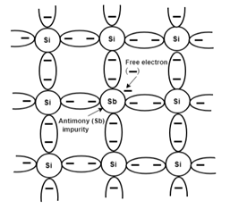 Figure 3. N-type semiconductor with donor impurityP-type Semiconductors:P-type semiconductors are doped with the trivalent semiconductor. The trivalent impurities have 3 electrons in their valence shell. The examples of trivalent impurities include Boron (B), Gallium (G), Indium (In), Aluminium (Al). As depicted in figure 4, the dopant atom establishes covalent bonds with only three neighboring silicon atoms and a hole or vacancy is generated in the bond with the fourth silicon atom. The hole acts as a positive carrier or space for the electron to occupy. Thus the trivalent impurity has imparted a positive vacancy or hole which can readily accept electrons and hence it is called an Acceptor impurity.
 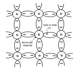 Figure 4. P-type semiconductor with the acceptor impurityCarrier Concentration in Intrinsic SemiconductorThe intrinsic carrier concentration is defined as the number of electrons per unit volume in the conduction band or the number of holes per unit volume in the valence band. Due to the applied voltage, the electron leaves the valence band and creates a positive hole in its place. This electron further enters the conduction band and takes part in the conduction of current. In an intrinsic semiconductor, the electrons generated in the conduction band is equal to the number of holes in the valence band. Therefore the electron concentration (n) is equal to the hole concentration (p) in an intrinsic semiconductor.Intrinsic carrier concentration can be given as:n_i=n=p Where,n_i : intrinsic carrier concentration n : electron-carrier concentration p : hole-carrier concentrationConductivity of Intrinsic SemiconductorAs the intrinsic semiconductor is subjected to heat or applied voltage the electrons travel from valence band to conduction band and leave a positive hole or vacancy in the valence band. Again these holes are filled by other electrons as more covalent bonds are broken. Thus the electrons and holes travel in the opposite direction and the intrinsic semiconductor starts conducting. The conductivity increases when a number of covalent bonds are broken thereby more electrons are holes are released for conduction. The conductivity of an intrinsic semiconductor is expressed in the terms of mobility and concentration of the charge carriers.The expression for the conductivity of an intrinsic semiconductor is given expressed as:σ_i=n_i e(μ_e+μ_h) Where σ_i: conductivity of an intrinsic semiconductor n_i : intrinsic carrier concentration μ_e: mobility of electrons μ_h: mobility of holesPlease refer to this link to know more about Semiconductor Theory MCQs
Leave a message
Message List
Comments Loading...