Products Category
- FM Transmitter
- 0-50w 50w-1000w 2kw-10kw 10kw+
- TV Transmitter
- 0-50w 50-1kw 2kw-10kw
- FM Antenna
- TV Antenna
- Antenna Accessory
- Cable Connector Power Splitter Dummy Load
- RF Transistor
- Power Supply
- Audio Equipments
- DTV Front End Equipment
- Link System
- STL system Microwave Link system
- FM Radio
- Power Meter
- Other Products
- Special for Coronavirus
Products Tags
Fmuser Sites
- es.fmuser.net
- it.fmuser.net
- fr.fmuser.net
- de.fmuser.net
- af.fmuser.net ->Afrikaans
- sq.fmuser.net ->Albanian
- ar.fmuser.net ->Arabic
- hy.fmuser.net ->Armenian
- az.fmuser.net ->Azerbaijani
- eu.fmuser.net ->Basque
- be.fmuser.net ->Belarusian
- bg.fmuser.net ->Bulgarian
- ca.fmuser.net ->Catalan
- zh-CN.fmuser.net ->Chinese (Simplified)
- zh-TW.fmuser.net ->Chinese (Traditional)
- hr.fmuser.net ->Croatian
- cs.fmuser.net ->Czech
- da.fmuser.net ->Danish
- nl.fmuser.net ->Dutch
- et.fmuser.net ->Estonian
- tl.fmuser.net ->Filipino
- fi.fmuser.net ->Finnish
- fr.fmuser.net ->French
- gl.fmuser.net ->Galician
- ka.fmuser.net ->Georgian
- de.fmuser.net ->German
- el.fmuser.net ->Greek
- ht.fmuser.net ->Haitian Creole
- iw.fmuser.net ->Hebrew
- hi.fmuser.net ->Hindi
- hu.fmuser.net ->Hungarian
- is.fmuser.net ->Icelandic
- id.fmuser.net ->Indonesian
- ga.fmuser.net ->Irish
- it.fmuser.net ->Italian
- ja.fmuser.net ->Japanese
- ko.fmuser.net ->Korean
- lv.fmuser.net ->Latvian
- lt.fmuser.net ->Lithuanian
- mk.fmuser.net ->Macedonian
- ms.fmuser.net ->Malay
- mt.fmuser.net ->Maltese
- no.fmuser.net ->Norwegian
- fa.fmuser.net ->Persian
- pl.fmuser.net ->Polish
- pt.fmuser.net ->Portuguese
- ro.fmuser.net ->Romanian
- ru.fmuser.net ->Russian
- sr.fmuser.net ->Serbian
- sk.fmuser.net ->Slovak
- sl.fmuser.net ->Slovenian
- es.fmuser.net ->Spanish
- sw.fmuser.net ->Swahili
- sv.fmuser.net ->Swedish
- th.fmuser.net ->Thai
- tr.fmuser.net ->Turkish
- uk.fmuser.net ->Ukrainian
- ur.fmuser.net ->Urdu
- vi.fmuser.net ->Vietnamese
- cy.fmuser.net ->Welsh
- yi.fmuser.net ->Yiddish
PCB Manufacturing Process | 16 Steps to Make a PCB Board

"PCB fabrication is very important in PCB industry, it is closely related to the PCB design, but do you really know the all the PCB fabrication steps in the PCB production? In this share, we will show you 16 steps in the PCB manufacturing process. Including what are they and how they work in the PCB fabrication process ----- FMUSER"
Sharing is Caring!
STEP 1: PCB Design - Designing and Output
STEP 2: PCB File Plotting - Film Generation of PCB Design
STEP 3: Inner layers Imaging Transfer - PRINT INNER LAYERS
STEP 4: Copper Etching - Removing the Unwanted Copper
STEP 5: Layer Alignment - Laminating the Layers Together
STEP 6: Holes Drilling - For Attaching the Components
STEP 7: Automated Optical Inspection (Multi-Layer PCB Only)
STEP 8: OXIDE (Multi-Layer PCB Only)
STEP 9: Outer layer Etching & Final Striping
STEP 10: Solder Mask, Silkscreen, and Surface Finishes
STEP 12: Electrical Test - Flying Probe Testing
STEP 13: Fabrication - Profiling and V-Scoring
STEP 14: Microsectioning - The Extra Step
STEP 15: Final inspection - PCB Quality Control
STEP 16: Packaging - Serves What You Need
Printed Circuit Board Design
Circuit board designing is the initial stage of the etching process while the CAM engineer stage is the first step in the PCB manufacturing of a new printed circuit board,The designer analyzes the requirement and selects the appropriate components such as processor, power supply, etc. Create a blueprint that fulfills all the requirements.

But, always remember that the circuit boards should be rigorously compatible with a PCB layout created by the designer using PCB design software. If you're a designer, you should inform your contract manufacturer about the PCB design software version used to design the circuit since it helps avoid issues caused by discrepancies before PCB fabrication.
Once the design is ready, get it printed on the transfer paper. Make sure that the design will fit inside the shiny side of the paper.
There are also many PCB terminology in PCB manufacturing, PCB design, and etc. You might have a better understanding of printed circuit board after reading some of the PCB terminologies from the below page!
Also read: PCB Terminology Glossary (Beginners-Friendly) | PCB Design
Usually, data arrives in a file format known as extended Gerber ( Gerber is also called RX274x), which is the most frequently used program, although other formats and databases can be used.
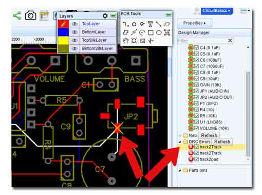
Once a design layout for the PCB is fed into the Gerber Extended software, all the different aspects of the design are looked over to ensure no errors.
After a thorough examination, the completed PCB design is taken to a PCB fabrication house for production. On arrival, the design undergoes a second check by the fabricator, known as a Design for Manufacture (DFM) check, which ensures:
● PCB design is manufacturable
● PCB design fulfills requirements for the minimum tolerances during the manufacturing process
▲ BACK ▲
Also Read: What is Printed Circuit Board (PCB) | All You Need to Know
STEP 2: PCB File Plotting - Film Generation of PCB Design
Once you have decided on your PCB design, the next step is to print it. This usually takes place in a temperature and humidity-controlled darkroom. Different layers of the PCB photo film are aligned by punching precise registration holes in each sheet of film. The film is created to help in creating a figure of the copper path.
Tips: As a PCB designer, after outputting your PCB schematic files, do not forget to remind the manufacturers to conduct a DFM check
A special printer called a laser photoplotter is commonly used in PCB printing, although it's a laser printer, it isn't a standard laserjet printer.
But this filming process is not adequate anymore for the miniaturization and technological advancements. It is becoming obsolete in some ways.
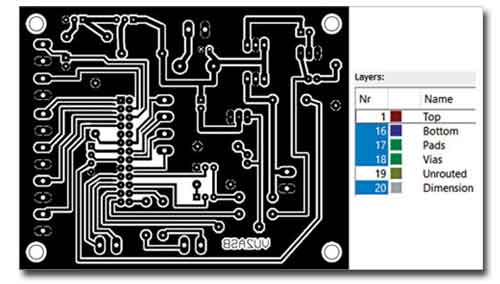
The laser photoplotter takes the board data and converts it into a pixel image, then a laser writes this onto the film and the exposed film is automatically developed and unloaded for the operator.
The final product results in a plastic sheet with a photo negative of the PCB in black ink. For the inner layers of PCB, black ink represents the conductive copper parts of the PCB. The remaining clear portion of the image denotes the areas of non-conductive material. The outer layers follow the opposite pattern: clear for copper, but black refers to the area that'll be etched away. The plotter automatically develops the film, and the film is securely stored to prevent any unwanted contact.
Each layer of PCB and solder mask receives its own clear and black film sheet. In total, a two-layer PCB needs four sheets: two for the layers and two for the solder mask. Significantly, all the films have to correspond perfectly to each other. When used in harmony, they map out the PCB alignment.
To achieve perfect alignment of all films, registration holes should be punched through all films. The exactness of the hole occurs by adjusting the table on which the film sits. When the tiny calibrations of the table lead to an optimal match, the hole is punched. The holes will fit into the registration pins in the next step of the imaging process.
Also read: Through Hole vs Surface Mount | What is the Difference?
▲ BACK ▲
This step only applies to boards with more than two layers. Simple two-layer boards skip ahead to drilling. Multiple-layer boards require more steps.
The first step is to clean the copper.
In PCB construction, cleanliness does matter. The copper-sided laminate is cleaned and passed into a decontaminated environment. Always remember to make sure that no dust gets onto the surface where it could cause a short or open circuit on the finished PCB.
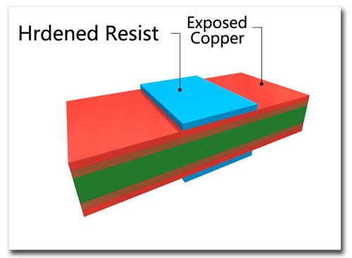
The clean panel receives a layer of a photo-sensitive film called photoresist. The printer uses powerful UV lamps which harden the photoresist through the clear film to define the copper pattern.
This ensures an exact match from the photo films to the photoresist.
The operator loads the first film onto the pins, then the coated panel then the second film. The bed of the printer has registration pins matching the holes in the photo tools and in the panel, ensuring that the top and bottom layers are precisely aligned.
The film and board line up and receive a blast of UV light. The light passes through the clear parts of the film, hardening the photoresist on the copper underneath. The black ink from the plotter prevents the light from reaching the areas not meant to harden, and they are slated for removal.
Under the black areas, the resistance remains unhardened. The cleanroom uses yellow lighting as the photoresist is sensitive to UV light.
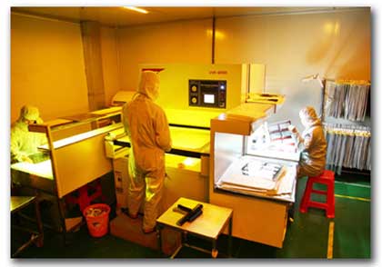
The product emerges with resistance properly covering the copper areas meant to remain in the final form. A technician examines the boards to ensure that no errors occur during this stage. All the resist present at this point denotes the copper that will emerge in the finished PCB.
Also read: PCB Design | PCB Manufacturing Process Flow Chart, PPT, and PDF
▲ BACK ▲
STEP 4: Copper Etching - Removing the Unwanted Copper
In PCB fabrication, etching is a process of removal of unwanted copper (Cu) from the circuit board. The unwanted copper is nothing but the non-circuit copper that is removed from the board. As a result, the desired circuit pattern is achieved. During this process, the base copper or the start copper is removed from the board.
The unhardened photoresist is removed and the hardened resist protects the desired copper, the board proceeds to unwanted copper removal. We use acidic etchant to wash off the excess copper. Meanwhile, the copper we wish to keep remains fully covered beneath the layer of photo-resist.
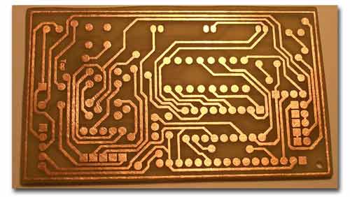
The PCB manufacturers usually employ a wet etching process. In wet etching, the unwanted material gets dissolved when immersed in a chemical solution.
There are two methods of wet etching:
● Alkaline etching (Ammoniacal)
The acidic method is used to etch off the inner layers in a PCB. This method involves chemical solvents like Ferric chloride (FeCl3) OR Cupric Chloride (CuCl2).
The alkaline method is used to etch off the outer layers in a PCB. Here, the chemicals utilized are chloride copper (CuCl2 Castle, 2H2O) + hydrochloride (HCl) + hydrogen peroxide (H2O2) + water (H2O) composition. The alkaline method is a fast process and is a bit expensive.
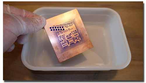
The process is carefully controlled to ensure that the finished conductor widths are exactly as designed. But designers should be aware that thicker copper foils need wider spaces between the tracks. The operator checks carefully that all the unwanted copper has been etched away
Once the unwanted copper is removed, the board is processed for stripping where the tin or tin/lean or the photoresist is removed from the board.
Now, unwanted copper is removed with the help of a chemical solution. This solution will remove extra copper without harming the hardened photoresist.
Also read: How to Recycle A Waste Printed Circuit Board? | Things You Should Know
▲ BACK ▲
STEP 5: Layer Alignment - Laminating the Layers Together
Together with thin layers of copper foil to cover the external surfaces of the top and bottom sides of the board, layer pairs are stacked to create a PCB “sandwich.” To facilitate the bonding of the layers, each layer pair will have a sheet of “prepreg” inserted between them. Prepreg is a fiberglass material impregnated with epoxy resin that will melt during the heat and pressure of the lamination process. As the prepreg cools, it will bond the layer pairs together.
To produce a multi-layer PCB, alternating layers of epoxy-infused fiberglass sheet called prepreg and conductive core materials are laminated together under high temperature and pressure using a hydraulic press. The pressure and heat cause the prepreg to melt and join the layers together. After cooling, the resulting material follows the same manufacturing processes as a double-sided PCB. Here’s more detail on the lamination process using a 4-layer PCB as an example:

Compositing the board together during this phase requires a lot of attention to detail to maintain the correct alignment of the circuitry on the different layers. Once the stack is complete the sandwiched layers are laminated, and the heat and pressure of the lamination process will fuse the layers together into one circuit board.
▲ BACK ▲
STEP 6: Holes Drilling - For Attaching the Components
Vias, mounting, and other holes are drilled through the PCB (usually in panel stacks, depending on the depth of the drill). Accuracy and clean hole walls are essential, and sophisticated optics provide this.
To find the location of the drill targets, an x-ray locator identifies the proper drill target spots. Then, proper registration holes are bored to secure the stack for the series of more specific holes.
Before drilling, the technician places a board of buffer material beneath the drill target to ensure a clean bore is enacted. The exit-material prevents any unnecessary tearing upon the drill's exits.
A computer controls every micro-movement of the drill - it's only natural that a product that determines the behavior of machines would rely on computers. The computer-driven machine uses the drilling file from the original design to identify the proper spots to bore.
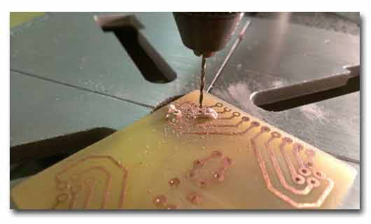
Once holes are drilled they get cleaned using chemical and mechanical processes to remove resin smears and debris caused by drilling. The entire exposed surface of the board, including the interior of the holes, is then chemically coated with a thin layer of copper. This creates a metallic base for electroplating additional copper into the holes and onto the surface in the next step.
After the drilling completes itself, the additional copper that lines the edges of the production panel undergoes removal by a profiling tool.
▲ BACK ▲
STEP 7: Automated Optical Inspection (Multi-Layer PCB Only)
After lamination, it is impossible to sort out errors in inner layers. Hence the panel is subjected to automatic optical inspection before bonding up and lamination. The machine scans the layers using a laser sensor and compares it with the original Gerber file to list out discrepancies, if any.
After all the layers are clean and ready, they need to be inspected for alignment. Both the inner and outers layers will be lined up with the help of holes drilled earlier. An optical punch machine drills a pin over the holes to keep layers aligned. After this, the inspection process starts to make sure there are no imperfections.
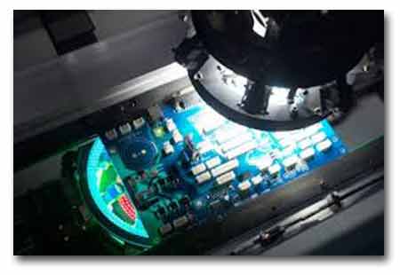
The most common events that occur during the layer image process that result in a short or open related issue are:
● Image is exposed incorrectly, causing either an increase/decrease in the size of features.
● The poor dry film resists adhesion which can cause nicks, cuts, or pinholes in the etched pattern.
● Copper is under-etched, leaving unwanted copper or causing growth in feature size or shorts.
● Copper is over-etched, removing copper features that are necessary, creating reduced feature sizes or cuts.
Ultimately, AOI is an important part of the manufacturing process that helps ensure accuracy, quality, and on-time delivery of a PCB.
▲ BACK ▲
Oxide (called Black Oxide, or Brown Oxide depending on the process), is a chemical treatmento inner layers of multi-layer PCBs prior to lamination, for increasing the roughness of clad copper to improve laminate bond strength. This process helps prevent delamination, or, the separation between any of the layers of base material or between the laminate and the conductive foil, once the manufacturing process is complete.
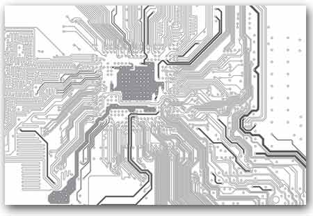
STEP 9: Outer layer Etching & Final Striping
Photoresist Stripping
Once the panel has been plated the photo-resist becomes undesirable and needs to be stripped from the panel. This is done in a horizontal process containing a pure alkaline solution that efficiently removes the photo-resist leaving the base copper of the panel exposed for removal in the following etching process.

The tin guards the ideal copper amid this stage. The undesirable exposed copper and copper underneath the rest of the resist layer experience removal. In this etching, we use ammoniacal etchant to etch off the undesirable copper. In the meantime, the tin secures the required copper during this stage.
The conducting regions and connections get legitimately settled at this stage.
Tin Stripping
Post etching process, the copper present on the PCB is covered by the etch resist, i.e., the tin, which is no more required. Therefore, we strip it off before proceeding further. You can use concentrated Nitric acid to remove the tin. Nitric acid is very effective in removing tin, and does not damage the copper circuit tracks below the tin metal. Thus, now you have a clear distinct outline of copper on the PCB.
Once the plating is complete on the panel, the dry film resists what remains and the copper that lies beneath needs to be removed. The panel will now go through the strip-etch-strip (SES) process. The panel is stripped of the resist and the copper that is now exposed and not covered by tin will be etched away so that only the traces and the pads around the holes and other copper patterns will remain. The dry film is removed from tin-plated panels and the exposed copper (not protected by tin) is etched away leaving the desired circuitry pattern. At this point, the fundamental circuitry of the board is completed
▲ BACK ▲
STEP 10: Solder Mask, Silkscreen, and Surface Finishes
To protect the board during assembly, the solder mask material is applied using a UV exposure process similar to what was used with the photoresist. This solder mask will cover the entire surface of the board except for the metal pads and features that will be soldered. In addition to the solder mask, component reference designators and other board markings are silk-screened onto the board. Both the solder mask and the silkscreen ink get cured by baking the circuit board in an oven.
The circuit board will also have a surface finish applied to its exposed metal surfaces. This helps to protect the exposed metal, and assists in the soldering operation during assembly. One example of a surface finish is hot air solder leveling (HASL). The board is first coated with flux to prepare it for the solder and then dipped into a bath of molten solder. As the board is removed from the solder bath, a high-pressure blast of hot air removes excess solder from the holes and smooths the solder on the surface metal.
The Solder Mask Application
A solder mask is applied to both sides of the board, but before that the panels are covered with an epoxy solder mask ink. The boards receive a flash of UV light, which passes through a solder mask. The covered portions remain unhardened and will undergo removal.
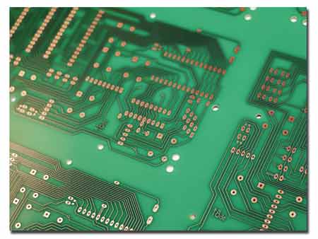
Green was chosen as the standard solder mask color because it doesn’t strain the eyes. Before machines could inspect PCBs during the manufacturing and assembling process, it was all manual inspections. The top light used for technicians to check the boards doesn’t reflect on a green solder mask and is best for their eyes.
The Nomenclature (silkscreen)
The silk-screening or profiling is the process of printing all of the critical information on the PCB, such as manufacturer id, company name component numbers, debugging points. This stands useful while servicing and repair.

It is also the most artistic process of PCB manufacturing. The almost completed board receives printing of human-readable letters, normally used to identify components, test points, PCB and PCBA part numbers, warning symbols, company logos, date codes, and manufacturer marks.
The PCB finally passes onto the last coating and curing stage.
The Gold or Silver surface finish
The PCB is plated with gold or silver to add extra solder-ability to the board, which will increase the bond of the solder.
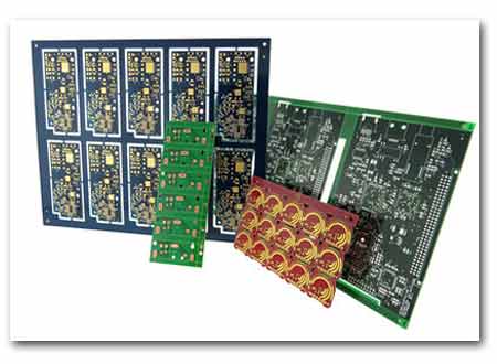
The application of each surface finish may vary slightly in the process but involves dipping the panel into a chemical bath to coat any exposed copper with the desired finish.
The final chemical process used to manufacture a PCB is applying the surface finish. While the solder mask covers most of the circuitry, the surface finish is designed to prevent oxidation of the remaining exposed copper. This is important because oxidized copper cannot be soldered. There are many different surface finishes that can be applied to a circuit board. The most common is Hot Air Solder Level (HASL), which is offered as both led and lead-free. But depending on the PCB’s specifications, application, or assembly process, suitable surface finishes may include Electroless Nickel Immersion Gold (ENIG), Soft Gold, Hard Gold, Immersion Silver, Immersion Tin, Organic Solderability Preservative (OSP), and others.
The PCB is then plated with a gold, silver, or lead-free HASL or hot air solder leveling finish. This is done so that the components are able to be soldered to the pads created and to protect the copper.
▲ BACK ▲
STEP 12: Electrical Test - Flying Probe Testing
As a final precaution for detection, the board will be tested by the technician for functionality. At this point, they use the automated procedure to confirm the functionality of the PCB and its conformity to the original design.
Usually, an advanced version of electrical testing called Flying Probe Testing which depends on moving probes to test the electrical performance of each net on a bare circuit board will be used in the electrical test.
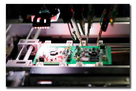
Any shorts or opens will be identified, enabling the operator to either make a repair or discard the PCB as defective. Depending on the complexity of the design and the number of test points, an electrical test may take anywhere from a few seconds to multiple hours to complete.
Also, depending on various factors such as complexity of the design, layer count, and component risk factor, some customers choose to forgo electrical testing to save some time and cost. This may be OK for simple double-sided PCBs where not many things can go wrong, but we always recommend electrical tests on multi-layer designs regardless of complexity. (Tip: Providing your manufacturer with a “netlist” in addition to your design files and fabrication notes is one way to prevent unexpected errors from occurring.)
▲ BACK ▲
STEP 13: Fabrication - Profiling and V-Scoring
Once a PCB panel has completed electrical testing, the individual boards are ready to be separated from the panel. This process is performed by a CNC machine, or Router, that routes each board out of the panel to the desired shape and size required. The router bits typically utilized are 0.030 - 0.093 in size and to speed the process, multiple panels can be stacked two or three high depending on the overall thickness of each. During this process, the CNC machine is also able to fabricate slots, chamfers, and beveled edges using a variety of different router bit sizes.
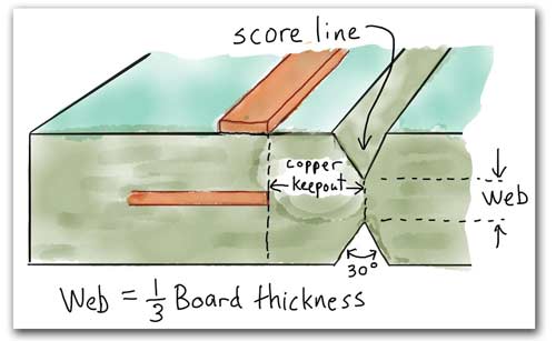
The routing process is a milling process in which a routing bit is used to cut the profile of the desired board contour. The panels are “pinned and stacked” as previously done during the “Drill” process. The usual stack is 1 to 4 panels.
To profile the PCBs and cut them out of the production panel, we need cutting, which is to cut different boards from the original panel. The method employed either center on using a router or a v-groove.A router leaves small tabs along the board edges while the v-groove cuts diagonal channels along both sides of the board. Both ways permit the boards to easily pop out from the panel.
Instead of routing individual small boards, the PCBs may be routed as arrays containing multiple boards with tabs or score lines. This allows for easier assembly of multiple boards at the same time while enabling the assembler to break apart the individual boards when the assembly is complete.
Lastly, the boards will be checked for cleanliness, sharp edges, burrs, etc, and cleaned up as needed.
STEP 14: Microsectioning - The Extra Step
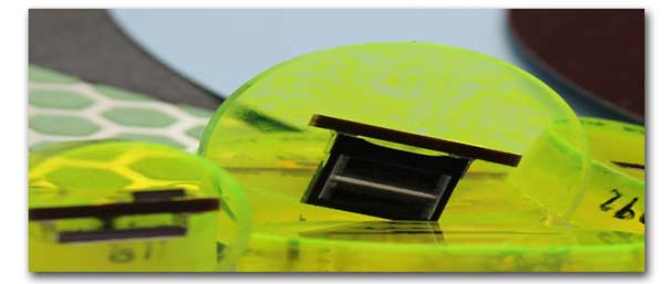
Micro sectioning (also known as a cross-section) is an optional step in the PCB manufacturing process but is a valuable tool used to validate the internal construction of a PCB for both verification and failure analysis purposes. To create a specimen for the microscopic examination of the material, a cross-section of the PCB is cut and placed into a soft acrylic that hardens around it in the shape of a hockey puck. The section is then polished and viewed under a microscope. A detailed inspection can be done by checking numerous details such as plating thicknesses, drill quality, and quality of internal interconnects.
STEP 15: Final inspection - PCB Quality Control
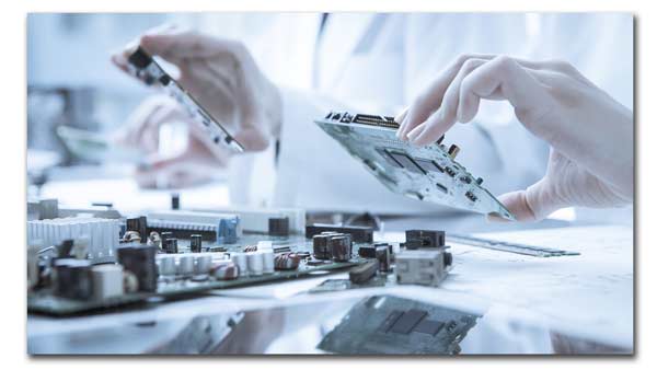
In the last step of the process, the inspectors should give each PCB a final careful check-over. Visual checking the PCB against acceptance criteria. Using manual visual inspection and AVI – compares PCB to Gerber and has a faster-checking speed than human eyes, but still requires human verification. All orders are also subjected to a full inspection including dimensional, solderability, etc to ensure the product meets our customer’s standards, and prior to pack and ship, a 100% quality audit is performed onboard lots.
● IPC-A-600 – Acceptability of Printed Boards, which defines an industry-wide quality standard for acceptance of PCBs.
● IPC-6012 – Qualification and Performance Specification for Rigid Boards, which establishes the types of rigid boards and describes the requirements to meet during fabrication for three performance classes of boards – Class 1, 2 & 3.
A Class 1 PCB would have a limited life and where the requirement is simply the function of the end-use product (ex. garage door opener).
A Class 2 PCB would be one where continued performance, extended life, and uninterrupted service is desired but not critical (ex. a PC motherboard).
A Class 3 PCB would include end-use where continued high performance or performance on demand is critical, failure cannot be tolerated, and the product must function when required (ex. flight control or defense systems).
▲ BACK ▲
STEP 16: Packaging - Serves What You Need
Boards are wrapped using materials that comply with the standard Packaging demands and then boxed prior to be being shipped using the requested mode of transport.
And as you might guess, the higher the class, the more expensive the PCB. In general, the difference between the classes is achieved by requiring tighter tolerances and controls that result in a more reliable product.
Regardless of the class specified, hole sizes are checked with pin gauges, the solder mask and legend are visually examined for overall appearance, the solder mask is checked to see if there is any encroachment on the pads, and the quality and coverage of the surface finish is examined.
IPC Inspection Guidelines and how they relate to the PCB design is very important to the PCB designers to become familiar with, the ordering and manufacturing process is vital as well.
Not all PCBs are created equal and understanding these guidelines will help ensure that the product produced meets your expectations for both aesthetics and performance.
If you're NEED ANY HELP with PCB design or have questions on the PCB manufacturing steps, please do not hesitate to share with FMUSER, We ARE ALWAYS LISTENING!
Sharing is Caring!
▲ BACK ▲

