
Products Category
- FM Transmitter
- 0-50w 50w-1000w 2kw-10kw 10kw+
- TV Transmitter
- 0-50w 50-1kw 2kw-10kw
- FM Antenna
- TV Antenna
- Antenna Accessory
- Cable Connector Power Splitter Dummy Load
- RF Transistor
- Power Supply
- Audio Equipments
- DTV Front End Equipment
- Link System
- STL system Microwave Link system
- FM Radio
- Power Meter
- Other Products
- Special for Coronavirus
Products Tags
Fmuser Sites
- es.fmuser.net
- it.fmuser.net
- fr.fmuser.net
- de.fmuser.net
- af.fmuser.net ->Afrikaans
- sq.fmuser.net ->Albanian
- ar.fmuser.net ->Arabic
- hy.fmuser.net ->Armenian
- az.fmuser.net ->Azerbaijani
- eu.fmuser.net ->Basque
- be.fmuser.net ->Belarusian
- bg.fmuser.net ->Bulgarian
- ca.fmuser.net ->Catalan
- zh-CN.fmuser.net ->Chinese (Simplified)
- zh-TW.fmuser.net ->Chinese (Traditional)
- hr.fmuser.net ->Croatian
- cs.fmuser.net ->Czech
- da.fmuser.net ->Danish
- nl.fmuser.net ->Dutch
- et.fmuser.net ->Estonian
- tl.fmuser.net ->Filipino
- fi.fmuser.net ->Finnish
- fr.fmuser.net ->French
- gl.fmuser.net ->Galician
- ka.fmuser.net ->Georgian
- de.fmuser.net ->German
- el.fmuser.net ->Greek
- ht.fmuser.net ->Haitian Creole
- iw.fmuser.net ->Hebrew
- hi.fmuser.net ->Hindi
- hu.fmuser.net ->Hungarian
- is.fmuser.net ->Icelandic
- id.fmuser.net ->Indonesian
- ga.fmuser.net ->Irish
- it.fmuser.net ->Italian
- ja.fmuser.net ->Japanese
- ko.fmuser.net ->Korean
- lv.fmuser.net ->Latvian
- lt.fmuser.net ->Lithuanian
- mk.fmuser.net ->Macedonian
- ms.fmuser.net ->Malay
- mt.fmuser.net ->Maltese
- no.fmuser.net ->Norwegian
- fa.fmuser.net ->Persian
- pl.fmuser.net ->Polish
- pt.fmuser.net ->Portuguese
- ro.fmuser.net ->Romanian
- ru.fmuser.net ->Russian
- sr.fmuser.net ->Serbian
- sk.fmuser.net ->Slovak
- sl.fmuser.net ->Slovenian
- es.fmuser.net ->Spanish
- sw.fmuser.net ->Swahili
- sv.fmuser.net ->Swedish
- th.fmuser.net ->Thai
- tr.fmuser.net ->Turkish
- uk.fmuser.net ->Ukrainian
- ur.fmuser.net ->Urdu
- vi.fmuser.net ->Vietnamese
- cy.fmuser.net ->Welsh
- yi.fmuser.net ->Yiddish
What is Gunn Diode : Construction & Its Working
Date:2021/10/18 21:55:58 Hits:
In GaAs semiconductor materials, the electrons are present in two states like high mass low velocity & low mass high velocity. By the demand of an adequate electric field, the electrons are forced to move from a low mass state to a high mass state. At this specific state, electrons can form a group & moves at a consistent rate that can cause to flow current in a series of pulses. So this is known as Gunn Effect which is used by Gunn diodes. These diodes are the best and most frequently available devices from the TED family (transferred electron devices). These types of diodes are used like DC to microwave converters with the negative resistance features of bulk GaAs (Gallium Arsenide) and they need a typical, stable voltage power supply, less impedance so that complex circuitry can be eliminated. This article discusses an overview of a Gunn diode.What is a Gunn Diode?Gunn diode is made with N-type semiconductor because it comprises majority charge carriers like electrons. This diode uses the negative resistance property to produce current at high frequencies. This diode is mainly used to produce microwave signals around 1 GHz & RF frequencies around 100 GHz. Gunn diodes are also known as TED (transferred electron devices). Even though it is a diode, the devices do not have a PN-junction but include an effect called the Gunn Effect. 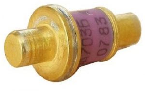 Gunn DiodeThis effect was named based on the inventor namely J B Gunn. These diodes are very simple to use, they form a low-cost technique to generate microwave RF signals, frequently being placed in a waveguide to make an easy resonant cavity. The Gunn diode symbol is shown below.
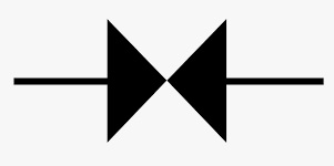 Symbol Gunn Diode ConstructionThe fabrication of the Gunn diode can be done with an N-type semiconductor. The materials which are used most frequently are GaAs (gallium Arsenide) & InP (Indium Phosphide) and other materials have been utilized like Ge, ZnSe, InAs, CdTe, InSb.It is essential to utilize n-type material because the effect of the transferred electron is simply appropriate to electrons & not holes found in a p-type material. In this device, there are 3 main regions which are called top, bottom & middle areas.
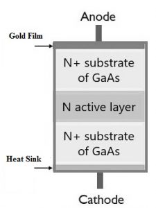 ConstructionThe general method to manufacture this diode is to grow & epitaxial layer on a degenerate n+ substrate. The thickness of the active layer ranges from few microns to 100 microns and the doping level of this layer ranges from 1014cm-3 to 1016cm-3. But this doping level is significantly low which is used for the top & bottom regions of the device. Based on the required frequency, the thickness will change. The deposition of the n+ layer can be done epitaxially otherwise doped through ion implantation. Both the areas of this device like top & bottom are doped deeply to provide n+ material. This gives the necessary high conductivity regions that are required for the connections toward the device.Generally, these devices are placed on conducting support to which the connection of a wire is made. This support can also work like a heat sink which is dangerous to remove the heat. The diode’s other terminal connection can be made through a gold connection that is deposited onto the pinnacle surface. Here the gold connection is necessary due to its high conductivity & relative stability. While manufacturing, the material device should be defect-free & also include an extremely consistent range of doping.Gunn Diode WorkingThe working principle of a Gunn diode mainly depends on the Gunn Effect. In some materials like InP & GaAs, once a threshold level is attained through an electric field within the material, then electrons mobility will decrease concurrently. When the electric field enhances then negative resistance will be generated.Once the intensity of an electric field for GaAs material reaches its significant value on the negative electrode, then low electron mobility region can be formed. This region moves through the average electrons speed to the +Ve electrode.Gunn diode includes a negative resistance region on its CV characteristics. Once the significant value is attained through the negative GaAs electrode, then there will be a region through the mobility of low electrons. After that, it will shift to the positive electrode. Once it meets a strong electric field domain through the positive electrode on the negative electrode, then a cyclic type of the region for less electron mobility as well as the high electric field will begin to re-create. The cyclical nature of this incident produces oscillations with 100 GHz frequencies. Once this value exceeds, then oscillations will begin to disappear quickly.CharacteristicsThe Gunn diode characteristics show a negative resistance area on its VI characteristic curve shown below. So this region allows the diode to amplify signals, so it can be used in oscillators & amplifiers. But, the Gunn diode oscillators are used most frequently.
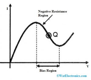 Characteristics of Gunn DiodeHere, the negative resistance area in the Gunn diode is nothing but once the flow of current increases then the voltage drops. This phase reverse allows the diode to work like an oscillator & an amplifier. The flow of current in this diode increases through the DC voltage. At a specific end, the flow of current will start decreasing, so this is called a peak point or threshold point. Once the threshold point is crossed then the flow of current will start reducing to create a negative resistance region within the diode.Modes of Operation of Gunn DiodeThe operation of a Gunn diode can be done in four modes which include the following.Gunn Oscillation ModeStable Amplification ModeLSA Oscillation ModeBias Circuit Oscillation ModeGunn Oscillation ModeGunn oscillation mode can be defined in the area wherever the sum of frequency can be multiplied by 107 cm/s lengths. The sum of doping can be multiplied through the length is higher than 1012/cm2. In this region, the diode is not stable due to the formation of cyclic either the high field domain & the accumulation layer.Stable Amplification ModeThis kind of mode can be defined in the area wherever the sum of frequency times length is 107cm/sec & the doping product length for time ranges from 1011 & 1012/cm2.LSA Oscillation ModeThis kind of mode can be defined in the area where the sum of times length of frequency is 107 cm/s & the doping quotient can be divided through the frequency is ranges from 2×10⁴ & 2×10⁵.Bias Circuit Oscillation ModeThis kind of mode happens simply once there is either LSA or Gunn oscillation takes place. Generally, it is the area wherever the time’s length product of frequency is very small to appear within the figure. Once the biasing of a bulk diode is done to the threshold then the average current drops suddenly when the oscillation of Gunn starts.Gunn Diode Oscillator CircuitThe circuit diagram of the Gunn diode oscillator circuit is shown below. The application of the Gunn diode diagram shows a negative resistance region. The negative resistance through stray capacitance and lead inductance can result in oscillations.
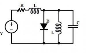 Gunn Diode Oscillator CircuitIn most cases, the relaxation kind of oscillations will include huge amplitude which will damage the diode. So a large capacitor is used across the diode to avoid this failure. This characteristic is mainly used to design oscillators at upper frequencies that range from GHz to THz bands. Here, the frequency can be controlled by adding a resonator. In the above circuit, the lumped circuit equivalent is a waveguide or coaxial transmission line.Here, GaAs Gunn diodes are accessible for operation which ranges from 10 GHz – 200 GHz at 5 MW – 65 MW power. These diodes can also be used as amplifiers.AdvantagesThe advantages of the Gunn diode include the following.This diode is available in small size & portableMaking the cost of this diode is lessAt high frequencies, this diode is stable & reliableIt possesses an improved noise-to-signal ratio (NSR) because it is protected from noise annoyance.It includes high bandwidthDisadvantagesThe disadvantages of the Gunn diode include the following.The temperature stability of this diode is poorThe operating current of this device, thus power dissipation is high.The Gunn diode efficiency is low under10GHz.Turn on the voltage of this device is highFM noise is high for specific applicationsThe range of tuning is highApplicationsThe applications of Gunn diode include the following.These diodes are used as oscillators & Amplifiers.It is used in microelectronics like control equipment.These are used in military, commercial radar sources & radio communication.This diode is used in pulsed Gunn diode generators.In microelectronics, these diodes are utilized as quick controlling devices for laser beam modulation.Used in police radars.These diodes are applicable in tachometersIt is used as pump sources within parametric amplifiersUsed in sensors to detect different systems like a door opening, trespass detecting & pedestrian safety, etc.It is used in nonstop wave doppler radars.It is used widely in transmitters of microwave relay data linkIt is used in electronics oscillators for generating microwave frequenciesThus, this is all about an overview of Gunn diode and its working. These types of diodes are also called TED (Transferred Electronic Device). Generally, these are used for high-frequency oscillations. Here is a question for you, what is Gunn Effect?
Leave a message
Message List
Comments Loading...