
Products Category
- FM Transmitter
- 0-50w 50w-1000w 2kw-10kw 10kw+
- TV Transmitter
- 0-50w 50-1kw 2kw-10kw
- FM Antenna
- TV Antenna
- Antenna Accessory
- Cable Connector Power Splitter Dummy Load
- RF Transistor
- Power Supply
- Audio Equipments
- DTV Front End Equipment
- Link System
- STL system Microwave Link system
- FM Radio
- Power Meter
- Other Products
- Special for Coronavirus
Products Tags
Fmuser Sites
- es.fmuser.net
- it.fmuser.net
- fr.fmuser.net
- de.fmuser.net
- af.fmuser.net ->Afrikaans
- sq.fmuser.net ->Albanian
- ar.fmuser.net ->Arabic
- hy.fmuser.net ->Armenian
- az.fmuser.net ->Azerbaijani
- eu.fmuser.net ->Basque
- be.fmuser.net ->Belarusian
- bg.fmuser.net ->Bulgarian
- ca.fmuser.net ->Catalan
- zh-CN.fmuser.net ->Chinese (Simplified)
- zh-TW.fmuser.net ->Chinese (Traditional)
- hr.fmuser.net ->Croatian
- cs.fmuser.net ->Czech
- da.fmuser.net ->Danish
- nl.fmuser.net ->Dutch
- et.fmuser.net ->Estonian
- tl.fmuser.net ->Filipino
- fi.fmuser.net ->Finnish
- fr.fmuser.net ->French
- gl.fmuser.net ->Galician
- ka.fmuser.net ->Georgian
- de.fmuser.net ->German
- el.fmuser.net ->Greek
- ht.fmuser.net ->Haitian Creole
- iw.fmuser.net ->Hebrew
- hi.fmuser.net ->Hindi
- hu.fmuser.net ->Hungarian
- is.fmuser.net ->Icelandic
- id.fmuser.net ->Indonesian
- ga.fmuser.net ->Irish
- it.fmuser.net ->Italian
- ja.fmuser.net ->Japanese
- ko.fmuser.net ->Korean
- lv.fmuser.net ->Latvian
- lt.fmuser.net ->Lithuanian
- mk.fmuser.net ->Macedonian
- ms.fmuser.net ->Malay
- mt.fmuser.net ->Maltese
- no.fmuser.net ->Norwegian
- fa.fmuser.net ->Persian
- pl.fmuser.net ->Polish
- pt.fmuser.net ->Portuguese
- ro.fmuser.net ->Romanian
- ru.fmuser.net ->Russian
- sr.fmuser.net ->Serbian
- sk.fmuser.net ->Slovak
- sl.fmuser.net ->Slovenian
- es.fmuser.net ->Spanish
- sw.fmuser.net ->Swahili
- sv.fmuser.net ->Swedish
- th.fmuser.net ->Thai
- tr.fmuser.net ->Turkish
- uk.fmuser.net ->Ukrainian
- ur.fmuser.net ->Urdu
- vi.fmuser.net ->Vietnamese
- cy.fmuser.net ->Welsh
- yi.fmuser.net ->Yiddish
What is IMPATT Diode : Construction & Its Working
Date:2021/10/18 21:55:58 Hits:
The concept of IMPATT diode was actually invented in the year 1954 by William Shockley. So, he expanded the idea for producing a negative resistance with the help of a mechanism like transit time delay. He proposed the injection technique for charge carriers within a PN junction is forward biased and published his thought in the Technical Journal of Bell Systems in 1954 and titled with the name ‘Negative Resistance Occurring from Transit Time within Semiconductor Diodes.Further, the proposal was not extended until 1958 as Bell Laboratories implemented his P+ N I N+ diode structure and after that, it is called Read diode. After that in the year 1958, a technical journal was published with the title name “a proposed high-frequency, negative resistance diode.” In the year 1965, the first practical diode was made and observed first oscillations. The diode which is used for this demonstration was constructed through silicon with a P+ N structure. Later, the Read diode operation was verified & after that, a PIN diode was demonstrated in the year 1966 to work. What is IMPATT Diode?The full form of IMPATT diode is IMPatt ionization Avalanche Transit-Time. This is an extremely high-power diode used in microwave applications. Generally, it is used as an amplifier and oscillator at microwave frequencies. The operating frequency range of the IMPATT diode ranges from 3 – 100 GHz.Generally, this diode generates negative resistance characteristics so works as an oscillator at microwave frequencies for generating signals. This is mainly because of the transit time effect and impact ionization avalanche effect. The classification of IMPATT diodes can be done by two types namely single drift and double drift. Single drift devices are P+NN+, P+NIN+, N+PIP+, N+PP+.When we consider the P+NN+ device, the P+N junction is connected in reverse bias then it causes an avalanche breakdown that causes the region of P+ to inject into NN+ with a saturation velocity. But the holes injected from the region of NN+ do not drift which is called single drift devices. The best example of double drift devices is P+PNN+. In this kind of device, whenever the PN-junction is biased close to an avalanche breakdown, then the electron drift can be done through the NN+ region whereas the holes drift through the PP+ region which is known as double drift devices.FeaturesThe main features of the IMPATT diode include the following.Operating frequency ranges from 3GHz to 100GHThe working principle of the IMPATT diode is avalanche multiplicationOutput power is 1w CW & above 400watt pulsedEfficiency is 3% CW & 60% pulsed under 1GHzMore powerful as compared to GUNN diodeThe noise figure is 30dbIMPATT Diode Construction and WorkingThe construction of the IMPATT diode is shown below. This diode includes four regions like P+-N-I-N+. The structure of both the PIN diode and IMPATT is the same, but it works on an extremely high voltage gradient of approximately 400KV/cm to generate an avalanche current. Usually, different materials such as Si, GaAs, InP, or Ge are mainly used for its construction. But, material like GaAs is mostly preferred due to its less noise behavior.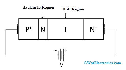 IMPATT Diode Construction As compared to a normal diode, this diode uses a somewhat different structure because; a normal diode will break down in an avalanche condition. As the huge amount of current generation causes the heat generation within it. So at microwave frequencies, deviation in structure is mainly used to generate RF signals. Generally, this diode is used in microwave generators. Here, a DC supply is given to the IMPATT diode to generate an output that oscillates once an appropriate tuned circuit is used within the circuit.The output of the IMPATT circuit is consistent & comparatively high as compared to other microwave diodes. But it also produces a high range of phase noise, which means that it is utilized in simple transmitters more commonly than local oscillators within receivers wherever the performance of phase noise is normally more significant.This diode works with fairly high voltage like70 volts or above. This diode can limit the applications through phase noise. Nevertheless, these diodes are mainly attractive alternatives for microwave diodes for several regions.IMPATT Diode Circuitapplication of IMPATT diode is shown below. Generally, this kind of diode is mainly used at above 3 GHz frequencies. It is noticed that whenever a tuned circuit is given with a voltage in the region of the breakdown voltage toward the IMPATT then oscillation will occur.As compared to other diodes, this diode uses negative resistance and this diode is capable of generating a high range of power typically ten watts or above based on the device. The operation of this diode can be done from a supply using a current limiting resistor. The value of this restricts the flow of current to the value necessary. The current is supplied throughout an RF choke to separate the DC from the RF signal.
 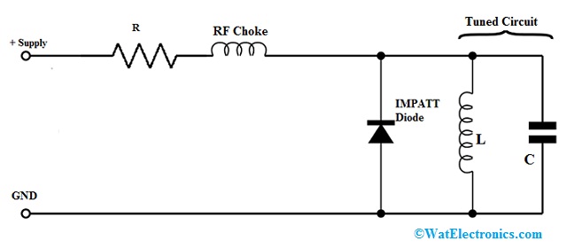 IMPATT Diode CircuitThe IMPATT microwave diode is arranged beyond the tuned circuit but normally this diode may be arranged within a waveguide cavity that gives the necessary tuned circuit. When the voltage supply is given then the circuit will swing.The main drawback of the IMPATT diode is its operation because it generates a high range of phase noise due to the mechanism of avalanche breakdown. These devices use Gallium Arsenide (GaAs) technology which is much better as compared to Silicon. This results from the very quicker ionization coefficients for charge carriers.Difference between IMPATT and Trapatt DiodeThe main difference between IMPATT and Trapatt diode based on different specifications is discussed below.SpecificationsIMPATT DiodeTRAPATT DiodeOperatingFrequency0.5 – 100GHz1 – 10GHzBandwidth1/10th of RF Center Frequency–Efficiency60% in pulsed mode & 3% in CWPulsed mode is 20 – 60%Output power1Watt(CW) 400Watt(Pulsed)Above 100 WattNoise Figure30 dB60 dBBasic semiconductorsSi, InP, Ge, GaAsSiConstructionN+PIP+ reverse bias PN JunctionP+ NN++ or N+ P P+ Reverse Bias PN JunctionHarmonicsLowStrongRuggednessYesYesSizeTinyTinyApplicationOscillator, AmplifierOscillatorIMPATT Diode CharacteristicsThe characteristics of the IMPATT diode include the following.It operates in reverse bias conditionThe materials used to manufacture these diodes are InP, Si & GaAs.These are compact & reliableIt generates a negative resistance area because of the effects of an avalanche as well as transit time.As compared to Gunn diodes, these provide high o/p power and noise also, so used in receivers for local oscillators.The phase difference between current and voltage is 180 degrees. Here phase delay with 90 degrees is mainly because of the avalanche effect whereas the remaining angle is because of transit time.These are mainly used where the high output power is necessary like oscillators & amplifiersThe output power provided by this diode is in the range of millimeter-wave frequency.At fewer frequencies, the output power is inversely proportional to frequencies whereas, at high frequencies, it is inversely proportional to the square of the frequency.AdvantagesThe advantages of the IMPATT diode include the following.It gives a high operating range.Its size is small.These are economical.At high temperature, it gives reliable operationAs compared to other diodes, it includes high power capabilities.Whenever it is used as an amplifier, then it works like a narrow band device.These diodes are used as excellent microwave generators.For the microwave transmission system, this diode can generate a carrier signal.DisadvantagesThe disadvantages of the IMPATT diode include the following.It gives a less tuning range.It gives high sensitivity to various operating conditions.In the avalanche region, the rate of electron-hole pair generation can cause a high noise generation.For operational conditions, it is responsive.If proper care is not taken then it may get damaged because of the huge electronic reactance.As compared to TRAPATT, it provides less efficiencyThe IMPATT diode’s tuning range is not good like the Gunn diode.It generates spurious noise through higher ranges as compared to Gunn & klystron diodes.ApplicationsThe applications of IMPATT diode include the following.These types of diodes are used like microwave oscillators within modulated output oscillators & microwave generators.These are used in continuous-wave radars, electronic countermeasures & microwave links.These are used for amplification through negative resistance.These diodes are used in parametric amplifiers, microwave oscillators, microwave generators. And also used in telecommunication transmitters, intruder alarm systems & receivers.Modulated Output OscillatorCW Doppler Radar TransmitterMicrowave GeneratorTransmitters of FM TelecommunicationReceiver LOIntrusion Alarm NetworkParametric AmplifierThus, this is all about an overview of IMPATT diode, construction, working, differences & its applications. These semiconductor devices are used for generating high-power microwave signals at a 3 GHz to 100 GHz range of frequencies. These diodes are applicable to fewer power alarms and radar systems. Here is a question for you, what is a TRAPATT diode?
Leave a message
Message List
Comments Loading...